Semiconductor device and method of manufacturing the same

A manufacturing method and semiconductor technology, applied in semiconductor/solid-state device manufacturing, semiconductor devices, transistors, etc., can solve problems such as the increase of current path resistance, and achieve the effect of avoiding resistance increase and easy depth control.

Inactive Publication Date: 2009-04-01
SANYO ELECTRIC CO LTD +1
View PDF0 Cites 9 Cited by
  • Summary
  • Abstract
  • Description
  • Claims
  • Application Information

AI Technical Summary

Problems solved by technology

Therefore, there is a problem that the resistance of the current path (especially the π portion 45) increases, and there is also a limit to the miniaturization of the n-type semiconductor region 22 and the p-type semiconductor region 23.

Method used


Image

  • Semiconductor device and method of manufacturing the same
  • Semiconductor device and method of manufacturing the same
  • Semiconductor device and method of manufacturing the same

Examples


Embodiment Construction

[0055] Refer below Figure 1 to Figure 12 , the embodiment of the present invention will be described by taking an n-channel MOSFET as an example.

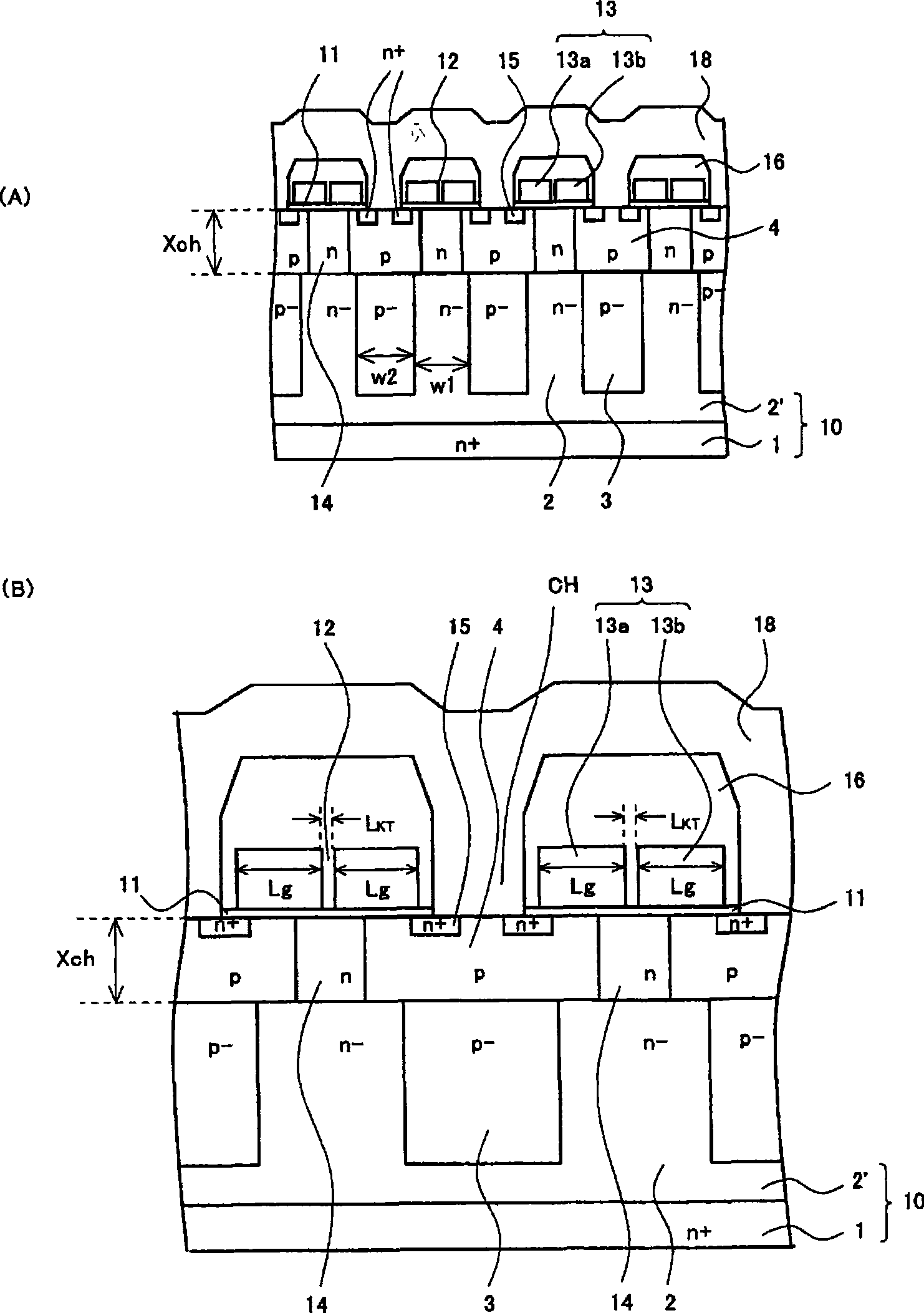
[0056] figure 1 It is a sectional view showing the structure of the MOSFET of this embodiment. figure 1 (A) is a sectional view showing a plurality of MOSFET cells, figure 1 (B) is figure 1 (A) Partial enlarged cross-sectional view.

[0057] The MOSFET has: a semiconductor substrate 1, a semiconductor region 2 of a conductivity type, a semiconductor region 3 of a reverse conductivity type, a channel region 4, an impurity region 14 of a conductivity type, a gate electrode 13, a gate insulating film 11, an interlayer insulating film 16, and source region 15 .

[0058] The substrate 10 has a super junction structure, and a plurality of columnar n-type semiconductor regions 2 and p-type semiconductor regions 3 are alternately arranged on the n+ type silicon semiconductor substrate 1 .

[0059] Here, the so-called super junct...


PUM


Abstract

Provided is a semiconductor device and a method of manufacturing a semiconductor device. In the semiconductor device, high-concentration n type impurity regions are formed respectively below gate electrodes. By setting a gate length to be smaller than a depth of channel regions, pn junction interfaces formed of adjacent side faces of the n type impurity regions and the channel regions can be substantially vertical to a top surface of a base. With this configuration, even when reduction in size is achieved in a super junction structure, a distance between the channel regions (i.e. a current path below the gate electrode) is not reduced unnecessarily. Accordingly, an increase in resistance can be prevented. In addition, depletion layers uniformly expand in the n type semiconductor regions, and impurity concentration of the regions can be increased consequently. Accordingly, reduction in resistance can be achieved.

Description

technical field [0001] The present invention relates to a semiconductor device and its manufacturing method, and more particularly to a semiconductor device capable of realizing high withstand voltage and low on-resistance and its manufacturing method. Background technique [0002] In a high-voltage power MOSFET (Metal Oxide Semiconductor Field Effect Transistor: Metal Oxide Semiconductor Field Effect Transistor) using semiconductor silicon, a high-resistance drift layer is provided in order to expand the depletion layer and relax the electric field when a reverse voltage is applied. . There is a technology that replaces the drift layer with a structure (super junction structure) in which columnar n-type semiconductor regions and p-type semiconductor regions with lower resistance than the drift layer are repeatedly arranged, thereby, compared with devices with conventional structures, Realization of low resistance (for example, refer to Patent Document 1). [0003] Refer b...

Claims


Application Information

Patent Timeline
Patent Type & Authority Applications(China)
IPC IPC(8): H01L27/088H01L29/78H01L29/06H01L29/423H01L21/8234H01L21/336H01L21/28
CPCH01L29/66712H01L29/1095H01L29/7802H01L29/42372H01L29/4238H01L29/0634H01L29/0878
Inventor 佐山康之
Owner SANYO ELECTRIC CO LTD
Why Eureka
Try Eureka