

Thin-film transistor and display device oxide semiconductor and gate dielectric having an oxygen concentration gradient
A technology of oxide semiconductors and thin film transistors, which is applied in the direction of transistors, semiconductor devices, semiconductor/solid-state device manufacturing, etc., and can solve the problems of uneven polycrystalline structure and interface inequality
- Summary
- Abstract
- Description
- Claims
- Application Information
AI Technical Summary
Problems solved by technology
Method used
Image

Examples
example 1
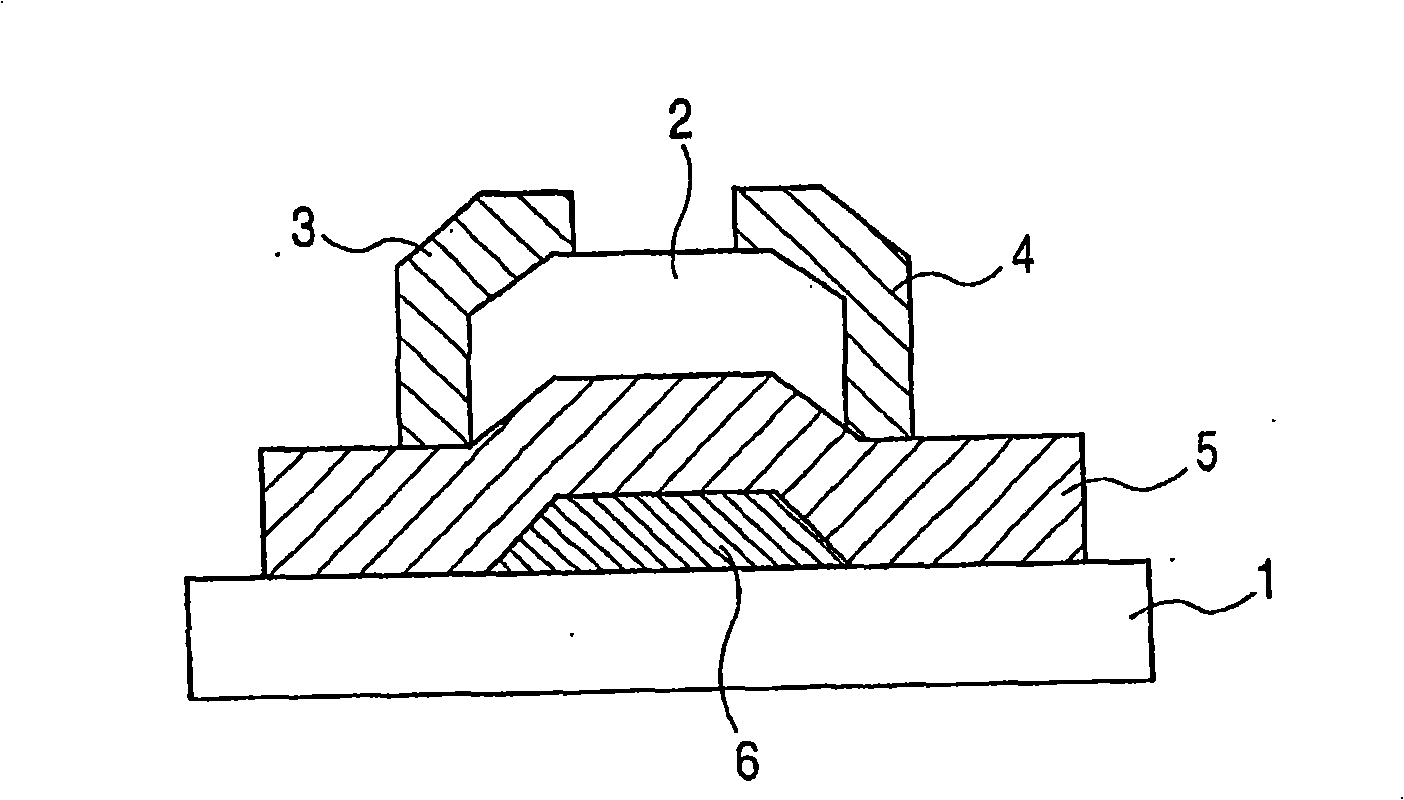
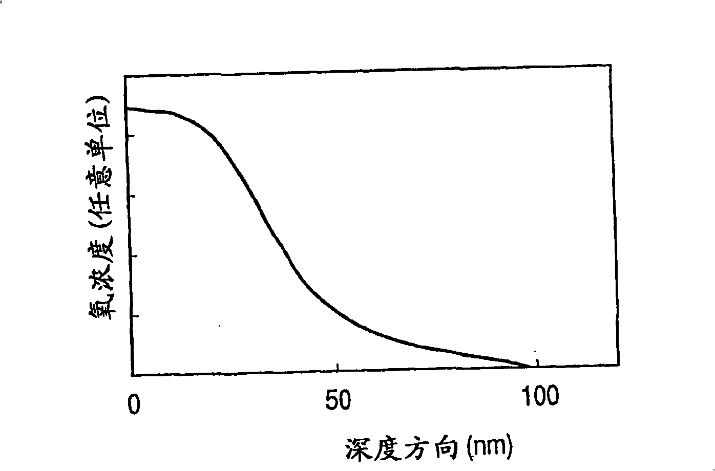
[0065] In this example, prepare figure 1 In the shown reverse staggered (bottom gate type) MISFET element, the amorphous silicon oxynitride used to form the gate insulating film has such an oxygen concentration distribution along its thickness direction that the oxygen concentration becomes high. First, a gate terminal having a thickness of Ti: 10 nm / Au: 100 nm was formed on a glass substrate using photolithography and lift-off. In addition, a-SiO with a thickness of 100 nm was formed thereon by sputtering x N y insulation layer. At this time, the Si 2 N 3 The target is used as a sputtering target, and the Ar / O 2 A mixed gas is used as a sputtering gas. change Ar / O 2 The oxygen concentration of the mixed gas is such that the insulating layer has the above-mentioned oxygen concentration distribution. Then, an amorphous oxide semiconductor film to be used as a channel layer was formed thereon to a thickness of 50 nm at room temperature by a sputtering method. Formed us...
example 2
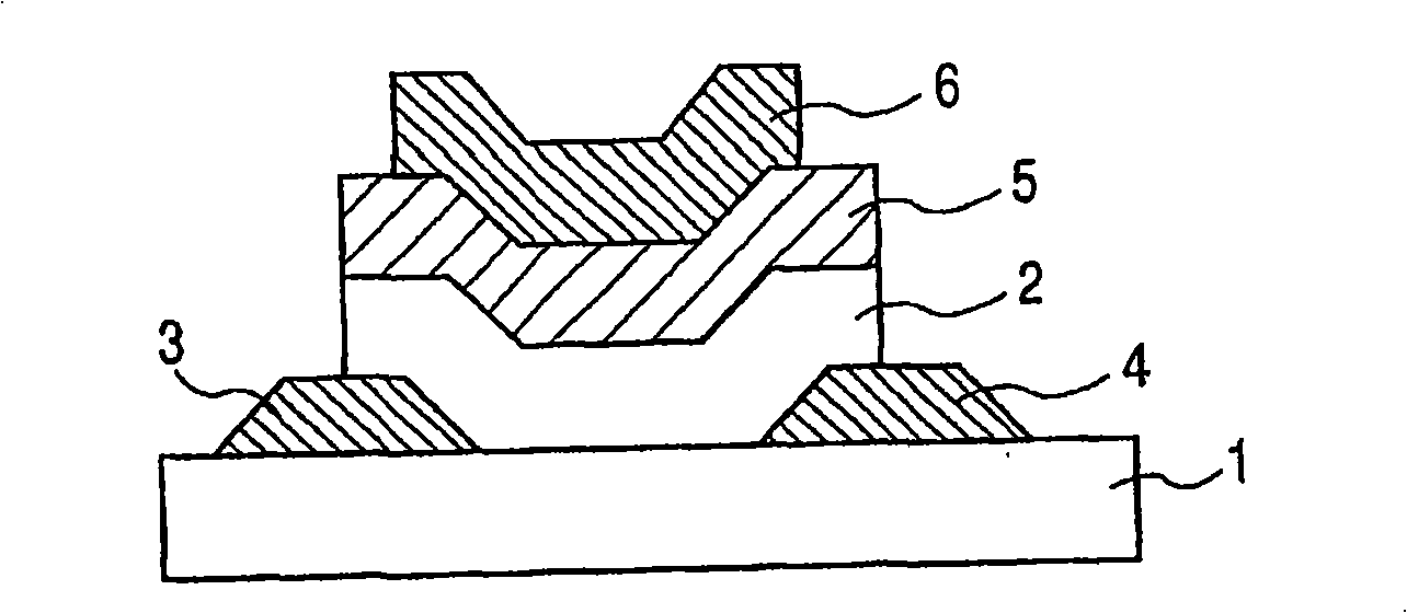
[0071] In this example, prepare figure 2 In the staggered (top gate) type MISFET element shown, first, a film having a thickness of Ti: 5nm / Au: 40nm is stacked on a glass substrate 1, and a drain terminal 4 and a source terminal are formed by photolithography and lift-off 3. An amorphous In-Ga-Zn-O film having a metal composition ratio of In:Ga:Zn=1.00:0.94:0.65 was formed with a thickness of 30 nm for the channel layer 2 by sputtering. In addition, 100nm thick a-SiO was formed on it by sputtering x N y The insulation layer 5. At this time, use Si 2 N 3 target as a sputtering target and using Ar / O 2 The mixed gas is used as the sputtering gas. By changing Ar / O 2 The oxygen concentration of the mixed gas causes the insulating layer to have an oxygen concentration distribution, so that the oxygen concentration of the insulating layer becomes higher on the interface side with the oxide semiconductor. Further, a film having a thickness of Ti: 5 nm / Au: 40 nm is stacked th...
example 3
[0075] In this example, the use of Figure 7 The TFT display device shown. The manufacturing process of this TFT is the same as that of Example 2. In the above TFT, the short side of the island of the ITO film for forming the drain electrode was extended to 100 μm, the extended 90 μm portion was left, and after wiring was fixed to the source and gate electrodes, the TFT was covered with an insulating layer. A polyimide film was coated thereon and the resultant was subjected to rubbing treatment. On the other hand, similarly, a plastic substrate on which an ITO film and a polyimide film were formed and subjected to rubbing treatment was prepared. This substrate was opposed to the above-prepared substrate on which the above-mentioned TFT was formed with a gap of 5 µm, and a nematic liquid crystal was injected into the gap. A pair of polarizing plates are further arranged on both sides of the structure. Here, when a voltage is applied to the source electrode of the TFT while ...
PUM
 Abstract
Description
Claims
Application Information