Method for preparing AlxIn1-xN film

A technology of alxin1-xn and thin film, which is applied in the field of preparation of nitride photoelectric thin film materials, can solve problems such as poor preferred orientation, and achieve the effects of good preferred orientation, stable deposition rate, and low sheet resistance

Inactive Publication Date: 2009-05-06
SICHUAN NORMAL UNIVERSITY
View PDF1 Cites 10 Cited by
  • Summary
  • Abstract
  • Description
  • Claims
  • Application Information

AI Technical Summary

Problems solved by technology

Peng et al. (Appl.Phys.Lett.1997, 71:17) grew a full range of polycrystalline Al directly on the substrate surface by sputtering x In 1-x N thin film (00.64 In 0.36 The N crystal structure is the best, but in its X-ray diffraction diagram, in addition to the (002) diffraction peak, there are also (102), (103) diffraction peaks appearing, and the preferred orientation is not good

Method used

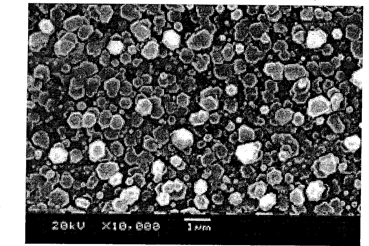
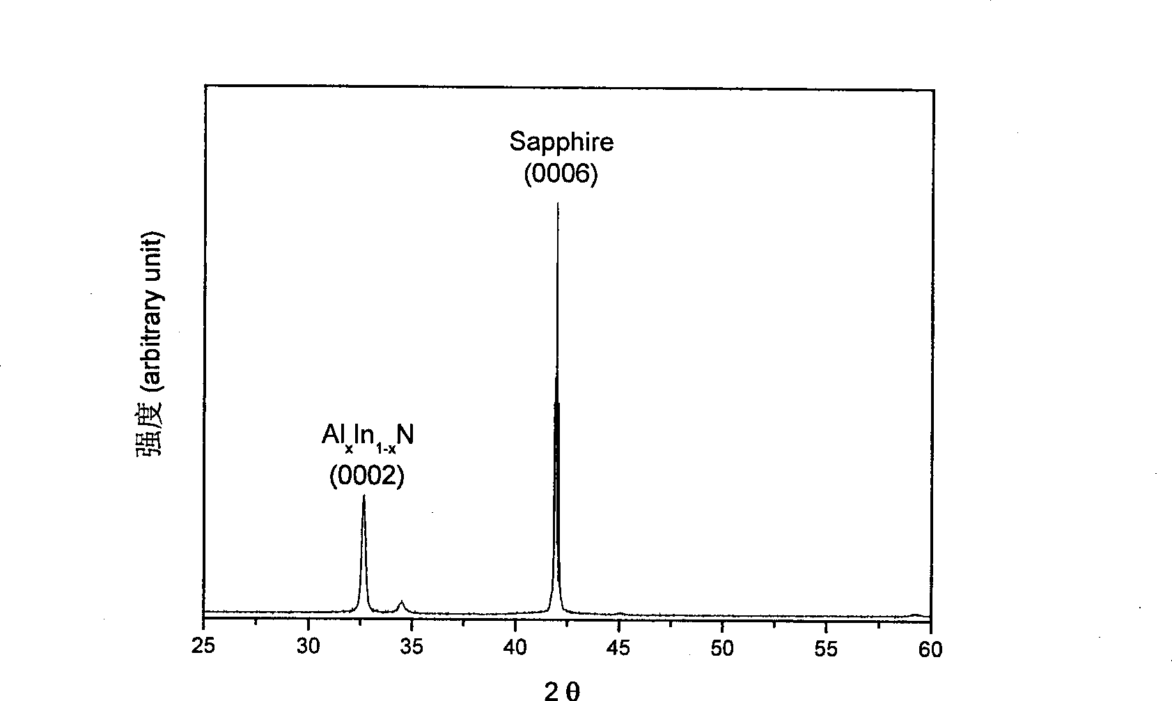
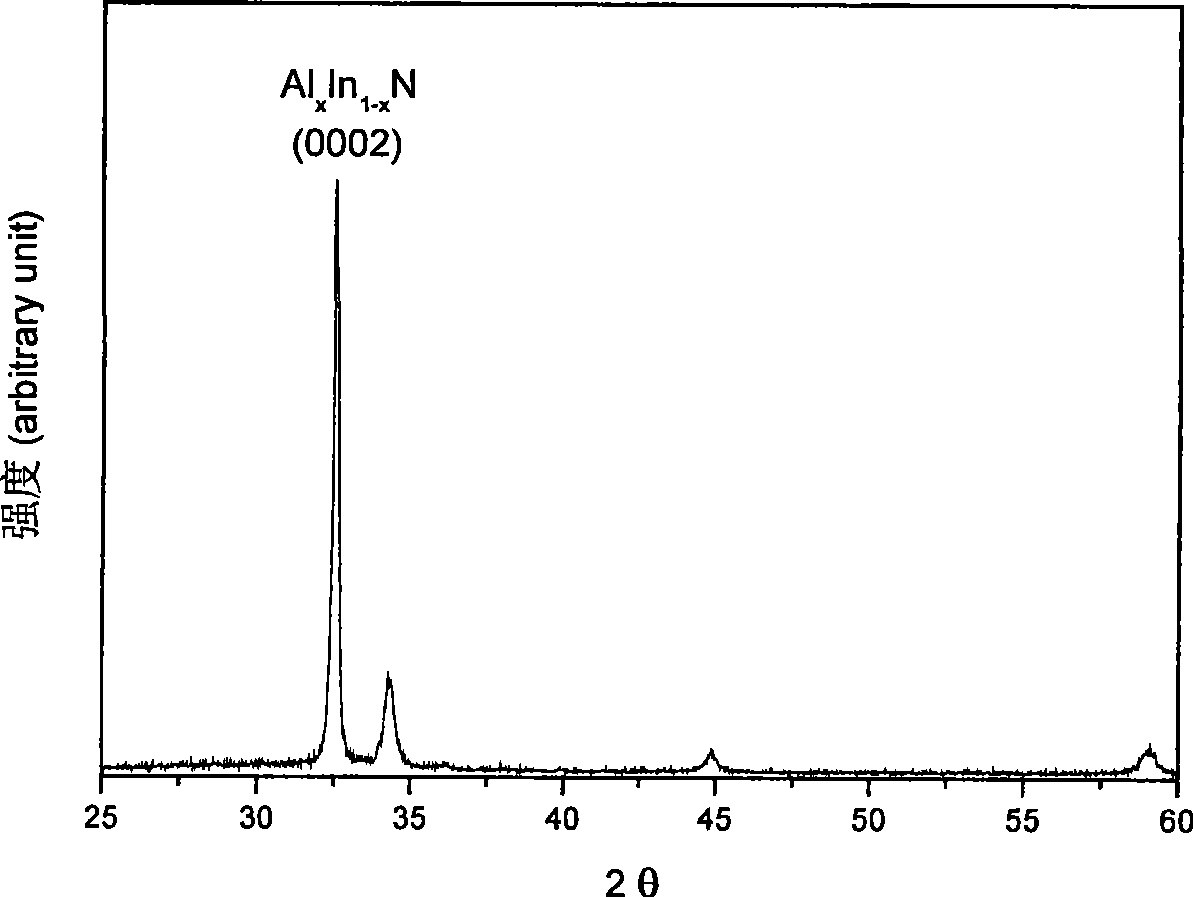

Image

  • Method for preparing AlxIn1-xN film
  • Method for preparing AlxIn1-xN film
  • Method for preparing AlxIn1-xN film

Examples


Embodiment 1

[0030] In this example, Al x In 1-x The preparation method of the N thin film operates according to the following process steps in sequence:

[0031] (1) Substrate processing

[0032] Using sapphire as the substrate, the sapphire substrate was ultrasonically cleaned in acetone for 30 minutes at room temperature and pressure, and then heated in H 2 SO 4 -H 3 PO 4 Solution (H2 SO 4 with H 3 PO 4 The volume ratio is 3:1) and boiled for 15 minutes, and then washed with deionized water for 10 minutes. After the substrate is cleaned, it is placed in a closed box and blown dry with nitrogen;

[0033] (2) Growth of buffer layer AlN

[0034] The growth of the buffer layer AlN was completed in an ultra-high vacuum multifunctional magnetron sputtering equipment (model: JGP560, manufacturer: Shenyang Scientific Instrument Development Center Co., Ltd., Chinese Academy of Sciences) with a background vacuum of 4.5×10 -5 Pa; the sapphire substrate processed through step (1) is put ...

Embodiment 2

[0040] In this example, Al x In 1-x The preparation method of the N thin film operates according to the following process steps in sequence:

[0041] (1) Substrate processing

[0042] Taking Si(111) as the substrate, at room temperature and pressure, the Si(111) substrate was first ultrasonically cleaned in trichlorethylene for 20 minutes, ultrasonically cleaned in acetone solution for 30 minutes, and then soaked in HF for 10 minutes , and then rinsed with deionized water for 10 minutes. After the substrate is cleaned, it is placed in a closed box and blown dry with nitrogen;

[0043] (2) Growth of buffer layer AlN

[0044] The growth of the buffer layer AlN is completed in an ultra-high vacuum multifunctional magnetron sputtering device (same as Example 1), and the background vacuum is 4.5 × 10 -5 Pa; the Si (111) substrate processed through step (1) is put into a sputtering chamber, and a buffer layer AlN is grown on the substrate by sputtering under vacuum conditions; ...

Embodiment 3

[0050] In this example, Al x In 1-x The preparation method of the N thin film operates according to the following process steps in sequence:

[0051] (1) Substrate processing

[0052] Using glass as a substrate, the glass substrate was firstly ultrasonically cleaned in acetone for 30 minutes, ultrasonically cleaned in absolute ethanol for 20 minutes, and then deionized water for 10 minutes at room temperature and pressure. After the substrate is cleaned, it is placed in a closed box and blown dry with nitrogen;

[0053] (2) Growth of buffer layer AlN

[0054] The growth of the buffer layer AlN is completed in an ultra-high vacuum multifunctional magnetron sputtering device (same as Example 1), and the background vacuum is 4.5 × 10 -5 Pa; put the glass substrate processed through step (1) into the sputtering chamber, and use the sputtering method to grow a buffer layer AlN on the substrate under vacuum conditions; the target material is Al (purity 99.8%), and the reaction g...


PUM

PropertyMeasurementUnit
particle sizeaaaaaaaaaa

Abstract

The invention discloses a method for preparing AlxIn1-xN thin films. The method comprises the following steps: (1) a substrate is completely cleaned by washing at normal temperature and normal pressure and placed in an atmosphere of nitrogen to be dried; (2) the treated substrate is placed in a sputtering chamber, and a buffer layer AIN is grown on the substrate under a vacuum condition by a sputtering method which uses Al as a target material and carries out sputtering for 20 to 30 minutes under conditions of a flow ratio of N2 to Ar of 1 to 9, a DC sputtering power of between 50 to 60w and the temperature of the substrate during sputtering controlled between 400 to 500 DEG C; and (3) after growth of the buffer layer AIN, the target material is changed into Al-In(1:1) alloy and an AlxIn1-xN thin film is grown under a vacuum condition by a sputtering method which carries out sputtering for 10 to 30 minutes under conditions of a flow ratio of N2 to Ar of 3 to 1, a DC sputtering power of between 80 to 160w and the temperature of the substrate during sputtering controlled between 250 to 350 DEG C.

Description

technical field [0001] The invention belongs to the field of preparation of nitride photoelectric thin film materials, in particular to an Al x In 1-x The preparation method of N thin film. Background technique [0002] Group III nitride semiconductor materials are considered to be the most potential optoelectronic materials because they have a wide adjustable direct band gap, especially with the advancement of experimental technology, the quality and performance of grown InN crystals have been greatly improved [China Patent 02145107.9], experimentally observed that the effective bandgap of InN film at room temperature is 0.7eV (Appl.Phys.Lett.2002, 80:3967-3969), making the direct bandgap of this group of semiconductor materials from 0.7eV (InN) Varying to 6.28eV (AlN), the smaller bandgap means that III-nitride-based optoelectronic devices emit light from the deep ultraviolet (AlN) to near-infrared (InN) region, thereby expanding their application in optoelectronic devic...

Claims


Application Information

Patent Timeline
Patent Type & Authority Applications(China)
IPC IPC(8): C23C14/34C23C14/06C23C14/54
Inventor 徐明董成军纪红萱陈青云魏屹
Owner SICHUAN NORMAL UNIVERSITY
Why Eureka
Try Eureka