
N type doping method for cubic boron nitride film

A cubic boron nitride and thin-film technology, which is applied in the fields of electrical components, semiconductor/solid-state device manufacturing, circuits, etc., can solve the problem that the doping dose is not easy to control, and achieve low cost, good portability, and room temperature resistivity. Reduced effect

Inactive Publication Date: 2011-08-10
INST OF SEMICONDUCTORS - CHINESE ACAD OF SCI
View PDF0 Cites 0 Cited by
  • Summary
  • Abstract
  • Description
  • Claims
  • Application Information

AI Technical Summary

Problems solved by technology

The common method of doping S into c-BN thin films is synchronous growth doping. Compared with ion implantation of S, synchronous growth doping puts forward higher requirements on equipment, and at the same time, the doping dose of S is not easy to control

Method used


Image

  • N type doping method for cubic boron nitride film
  • N type doping method for cubic boron nitride film
  • N type doping method for cubic boron nitride film

Examples


Embodiment Construction

[0022] In order to make the object, technical solution and advantages of the present invention clearer, the present invention will be described in further detail below in conjunction with specific embodiments and with reference to the accompanying drawings.

[0023] Growth process:

[0024] 1) The equipment used for growth is ion beam assisted deposition system, including deposition chamber, vacuum system, substrate heating and temperature control system, sample rotation system, ion source control system, etc.;

[0025] 2) Use high-purity B target as the sputtering target;

[0026] 3) The background vacuum of the sample chamber is 1×10 -5 Pa;

[0027] 4) First deposit c-BN film, the main ion source (Ar + Ion beam) process conditions are: beam current density J 1 360μA / cm 2 , ion energy U 1 1500eV; auxiliary ion source (Ar + +N 2 + The process condition of mixed ion beam) is: beam current density J 2 80μA / cm 2 , ion energy U 2 300eV, Ar + :N 2 + The beam ratio is...


PUM

PropertyMeasurementUnit
thicknessaaaaaaaaaa
electrical resistivityaaaaaaaaaa

Abstract

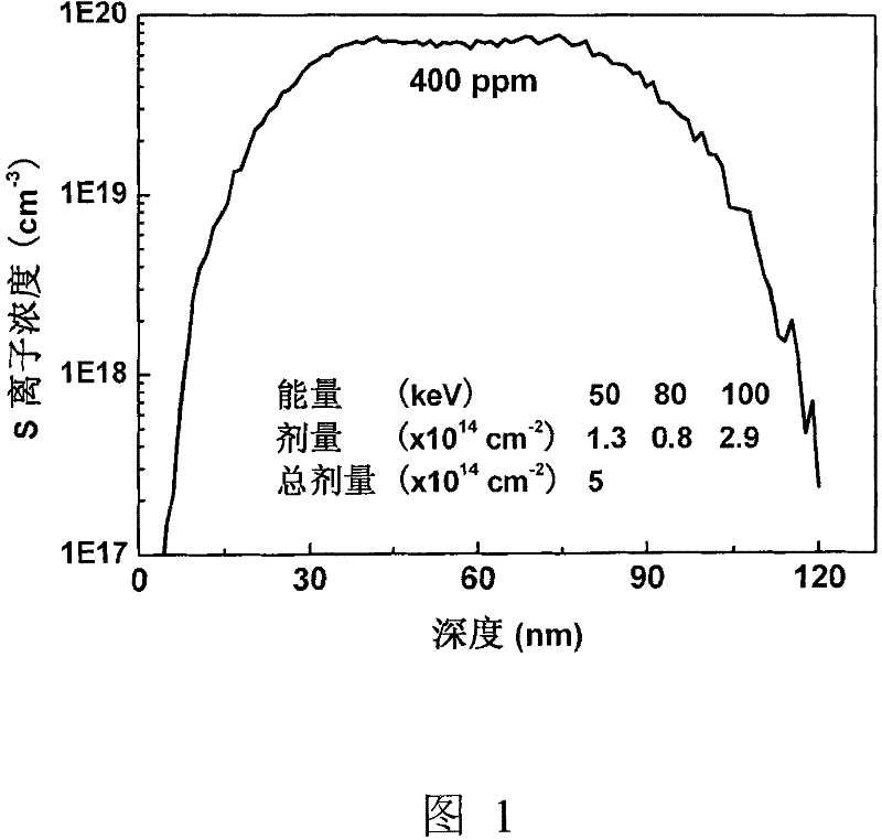
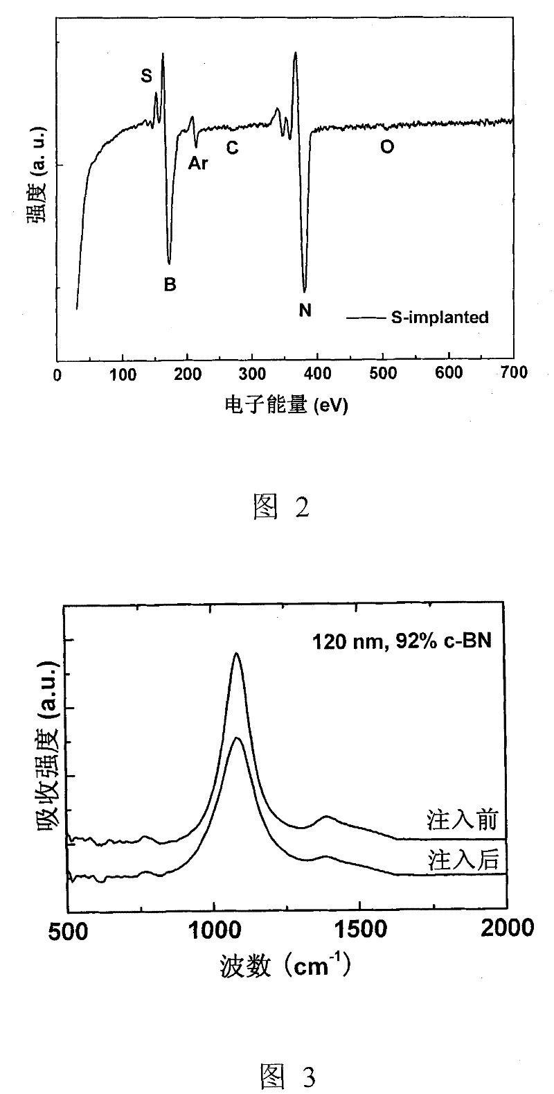
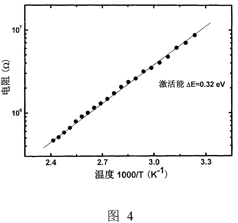
The invention relates to a method for n type doping of a cubic boron nitride(c-BN) film, which specifically comprises the following steps: firstly, using an Ion Beam Assisted Depostion (IBAD) method for preparing a high-quality c-BN film; secondly, sequentially injecting S ions with different energy (50, 80 and 100KeV) and total dose of 5*10<14>cm<-2> into the c-BN film; and finally achieving then type doping of the c-BN film. The method has no special requirement on growth equipment of the c-BN film, and has the advantages of capability of precisely controlling doping dose and dosing depth,low cost, convenient method, wide application, good portability and so on.

Description

technical field [0001] The invention relates to the technical field of semiconductors, in particular to a method for realizing n-type doping of a cubic boron nitride thin film. Background technique [0002] Cubic boron nitride (c-BN) is a III-V compound semiconductor material with superhardness, wide band gap, high thermal conductivity, high resistivity, high thermal stability and chemical stability. Together with diamond, silicon carbide and gallium nitride, it is called the third-generation semiconductor material after silicon, germanium and gallium arsenide. Among them, c-BN has the best comprehensive performance. It has broad application prospects in high-power electronic devices. The pure c-BN film is an insulator, which has the disadvantages of high resistivity and low carrier concentration, which limits its application in the field of microelectronic devices. Only by doping means to reduce its resistivity and increase carrier concentration can its application in the...

Claims


Application Information

Patent Timeline
Patent Type & Authority Patents(China)
IPC IPC(8): H01L21/18H01L21/203H01L21/265H01L21/324
Inventor 张兴旺范亚明陈诺夫
Owner INST OF SEMICONDUCTORS - CHINESE ACAD OF SCI
Learn More