Manufacturing method of gate-splitting type flash memory

A split-gate flash memory and manufacturing method technology, which is applied in semiconductor/solid-state device manufacturing, electrical components, electric solid-state devices, etc., can solve the problems that the control gate oxide layer cannot be thinned, and it is impossible to obtain the control gate oxide layer. The effect of reducing the thickness and enhancing the control ability

Active Publication Date: 2009-06-03
SHANGHAI HUAHONG GRACE SEMICON MFG CORP
View PDF0 Cites 27 Cited by
  • Summary
  • Abstract
  • Description
  • Claims
  • Application Information

AI Technical Summary

Problems solved by technology

The thicker the tunnel oxide layer is, the better the data retention ability of the floating gate is, so the tunnel oxide layer is required to reach a certain thickness. However, in the current process flow, the control gate oxide layer and the tunnel

Method used


Image

  • Manufacturing method of gate-splitting type flash memory
  • Manufacturing method of gate-splitting type flash memory
  • Manufacturing method of gate-splitting type flash memory

Examples


Embodiment Construction

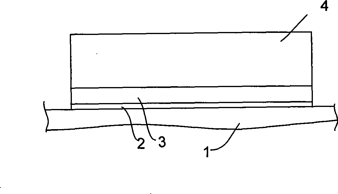
[0034] see Figure 1A As shown in the cross-sectional view of the manufacturing process, a single crystal silicon substrate 1 is provided, and the oxide layer 2 is thermally grown on the silicon substrate 1 to a thickness of about 70A to 150A. Optionally, the silicon substrate 1 Wherein is a P-type substrate and an N-type well is formed in the P-type substrate, or is an N-type substrate and a P-type well is formed in the N-type substrate. After the growth of the thermal oxide layer is completed, a second silicon layer 3 of polysilicon is formed on the oxide layer 2 with a thickness of 100A to 1000A, and a dielectric layer 4 is formed on the second silicon layer 3. The dielectric layer 4 It can be pure oxide or nitride. In this embodiment, the dielectric layer 4 is silicon nitride.

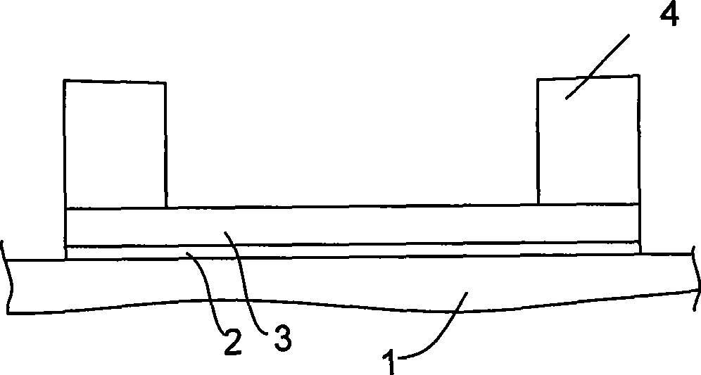
[0035] After completing the above-mentioned oxide layer 2, second silicon layer 3 and dielectric layer 4 processes, a photolithographic mask is formed on the surface of the dielectric layer 4, and...


PUM


Abstract

The invention discloses a manufacturing method of a gate-splitting type flash memory, which is characterized in that: the manufacturing method comprises the following steps: a first part of a tunneling oxide layer is formed on the side wall of a floating gate and the first part for controlling gate oxide layer is formed on an underlay of the floating gate; a second part of the tunneling oxide layer and the second part for controlling gate oxide layer are formed in a depositing manner; a first polysilicon layer is formed on the controlling gate oxide layer in a depositing manner; a side wall controlling gate is formed on the controlling gate oxide layer by etching an anisotropic polysilicon. The manufacturing method changes the controlling gate oxide layer and the tunneling oxide layer into the method that the grating type flash memory is formed by thermal oxygen oxidizing and CVD depositing and superimposing; namely, high-temperature oxidization is firstly carried out before CVD deposition, a gate oxide layer grows on the a monocrystalline silicon underlay and the tunneling oxide layer grows on the polysilicon floating gate; by utilizing the difference of the oxidizing velocity between the monocrystalline silicon and the polysilicon, the thickness of the controlling gate oxide layer is reduced, thus improving the controlling capacity of the controlling gate oxide layer to a channel and having no effect on the data holding capacity of the flash memory at the same time.

Description

technical field [0001] The invention relates to the field of chip manufacturing, in particular to a memory manufacturing method with a divided gate structure. Background technique [0002] Memory is used to store a large amount of digital information. According to recent surveys, memory chips account for about 30% of semiconductor transactions worldwide. Over the years, technological progress and market demand have led to more and more high-density various Types of memory, such as RAM (random access memory), DRAM (dynamic random access memory), ROM (read-only memory), EPROM (erasable programmable read-only memory), FLASH (flash memory) and FRAM (ferroelectric memory), etc. , flash memory or FLASH has become the mainstream of non-volatile semiconductor storage technology. Among various FLASH devices, they are basically divided into two types: stacked gate devices and split gate devices. Stacked gate devices have floating gates and The control gate, where the control gate is ...

Claims


Application Information

Patent Timeline
IPC IPC(8): H01L21/336H01L21/28H01L21/8247
CPCH01L27/11521H01L29/7881H01L29/42324H01L21/28273H01L29/40114H10B41/30
Inventor 董耀旗李荣林李栋徐爱斌
Owner SHANGHAI HUAHONG GRACE SEMICON MFG CORP
Why Eureka
Try Eureka