Polymer electroluminescent device and method for producing same

A technology of electroluminescent devices and polymers, which is applied in the direction of electric solid-state devices, semiconductor/solid-state device manufacturing, electrical components, etc., can solve the problems of unbalanced efficiency, low, carrier loss, etc., and achieve simple preparation process, Effects of improving efficiency performance and reducing losses

Inactive Publication Date: 2009-06-10
SOUTH CHINA UNIV OF TECH
View PDF18 Cites 10 Cited by
  • Summary
  • Abstract
  • Description
  • Claims
  • Application Information

AI Technical Summary

Problems solved by technology

[0015] The purpose of the present invention is to overcome the shortcomings of existing polymer electroluminescent devices with low efficiency due to carrier loss and imbalance, and to provide a polymer electroluminescent device and its preparation method

Method used


Image

  • Polymer electroluminescent device and method for producing same
  • Polymer electroluminescent device and method for producing same
  • Polymer electroluminescent device and method for producing same

Examples


Embodiment 1

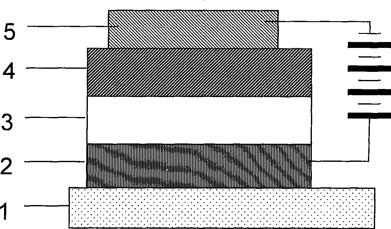
[0047] Select the high-resistance poly(3,4-dioxyethylthiophene)-poly(p-styrenesulfonic acid) purchased from H.C.STARCK company model as BAYTRON P CH 8000, and rotate it at a speed of 2000 rpm for 60 seconds to prepare A pre-coated anode buffer layer was obtained. The thickness of the anode buffer layer is 80 nanometers, the actual measured longitudinal resistance is (202±23) ohms, and the corresponding longitudinal resistivity is (4.29±0.49)×10 6 ohm cm. When mixing PEDOT:PSS (BAYTRON P CH 8000) and 1% glycerol aqueous solution with a mass concentration of 1:1 and 1:4 respectively, after the secondary film formation of the previously obtained high-resistance BAYTRON P CH8000, Its thickness is changed to 50 nanometers and 23 nanometers respectively, the normal resistance is measured to be (54.3±18.0) ohms and (16.4±3.5) ohms respectively, and the converted normal direction resistivity is (1.63±0.54)×10 6 Ohm cm sum (1.07±0.23)×10 5 ohm cm. In other words, the conductivity o...

Embodiment 2

[0061] Repeat Example 1, using p-type organic semiconductor and green light polymer polyphenylene substituted phenylene (P-PPV) as the light emitting layer, and other conditions remain unchanged. The effects of different anode buffer layers on the performance of polymer light-emitting devices based on polyphenylene-substituted styrene as the light-emitting layer are shown in Table 2.

[0062] Table 2

[0063]

[0064] Table 2 shows that the polymer electroluminescent device based on the anode buffer layer of high resistivity (with p-type conjugated polymer, green light-emitting material P-PPV as the light-emitting layer), can obtain more than the conventional device (BAYTRON P AI 4083) and higher current efficiency and external quantum efficiency of high-conductivity anode buffer layer devices (BAYTRON P).

Embodiment 3

[0066] It has been shown from Examples 1-2 that the device structure, method and anode buffer layer involved in the present invention are especially useful for polymer light-emitting devices (most of the light-emitting layer is a p-type semiconductor material) or p-type organic semiconductor-based doping type (doped Incorporating organometallic complexes) light-emitting devices have obvious effects. We also found that the high-resistivity anode buffer layer has the effect of further enhancing its performance (current efficiency, external quantum efficiency) for other high-efficiency p-type organic semiconductor-based doped (doped with organic metal complexes) light-emitting devices ( See the impact of different anode buffer layers in Table 3 on the performance of other doped (doped with organometallic complexes) light-emitting devices. Among the various device performance parameters in Table 3, the first row provides the corresponding current density-voltage- Performance; the ...


PUM

PropertyMeasurementUnit
thicknessaaaaaaaaaa
electrical resistivityaaaaaaaaaa
thicknessaaaaaaaaaa

Abstract

The invention provides a polymer electroluminescent device and a method for preparing the same. The device consists of a glass substrate, an anode, an anode buffer layer, a luminescent layer and a cathode which are cascaded sequentially; the preparation process of the anode buffer layer (3) comprises: the surface of the anode with metal conductivity is coated with a poly(3,4-dioxo-ethylthiophene)-poly(p-styrene sulfonate) aqueous suspension solution to form the anode buffer layer with thickness between 10 and 500 nanometers and high normal resistivity; and the poly(3,4-dioxo-ethylthiophene)-poly(p-styrene sulfonate) aqueous suspension solution is doped with polylol or a polar solvent and is coated on the anode buffer layer with high normal resistivity to obtain the anode buffer layer with normal resistivity between 1*10<5> and 2*10<6> ohm.centimeter and thickness between 1 and 100 nanometers. Compared with the prior device, the electroluminescent device has higher current efficiency, power efficiency and quantum efficiency.

Description

technical field [0001] The invention relates to the field of optoelectronic devices, in particular to the technical field of polymer electroluminescent devices (polymer light emitting diodes), in particular to a polymer electroluminescent device and a preparation method thereof. Background technique [0002] Organic light-emitting diodes (OLEDs) can be made of small molecules [US Patent 4,539,507], conjugated polymers [PCT International Patent WO 90 / 13148, PCT International Patent WO 95 / 06400 and PCT International Patent WO 99 / 48160] and dendrimers [PCT International Patent WO 99 / 21935 and PCT International Patent WO02 / 067343]. The simplest organic electroluminescent device structure is a single-layer sandwich structure (such as figure 2 shown), consisting of a glass substrate (1), anode (2), light-emitting layer (4) and cathode (5), the light-emitting layer (4) is sandwiched between two electrodes (anode (2) and cathode (5)) between. After an appropriate forward bias is...

Claims


Application Information

Patent Timeline
Patent Type & Authority Applications(China)
IPC IPC(8): H01L51/56
Inventor 吴宏滨邹建华安定杨伟曹镛
Owner SOUTH CHINA UNIV OF TECH
Why Eureka
Try Eureka