LED chip and preparation method thereof

A technology of LED chips and chips, applied in electrical components, circuits, semiconductor devices, etc., can solve problems such as limiting the external quantum efficiency of GaN-based light-emitting diodes, and achieve the effect of improving external quantum efficiency

Inactive Publication Date: 2009-07-01
深圳市方大国科光电技术有限公司
View PDF0 Cites 3 Cited by
  • Summary
  • Abstract
  • Description
  • Claims
  • Application Information

AI Technical Summary

Problems solved by technology

At present, all sides of commonly used LED chips are chamfered outwardly after etching, such as figure 1 As shown, since the reflection coefficients of GaN and air are 2.5 and 1 respectively, the critical angle at which the light generated in the InGaN-GaN active region can propagate is about 23°, and the light with an exit angle greater than 23° is in the InGaN-GaN active region. The chamfer-shaped sloped side outside the area produces total reflection, which is reflected back to the chip, which greatly limits the external quantum efficiency of GaN-based light-emitting diodes.

Method used


Image

  • LED chip and preparation method thereof
  • LED chip and preparation method thereof
  • LED chip and preparation method thereof

Examples


Embodiment 1

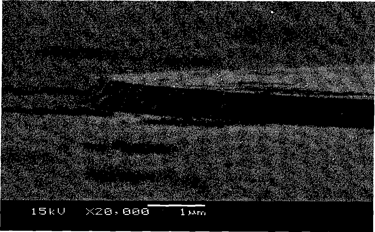
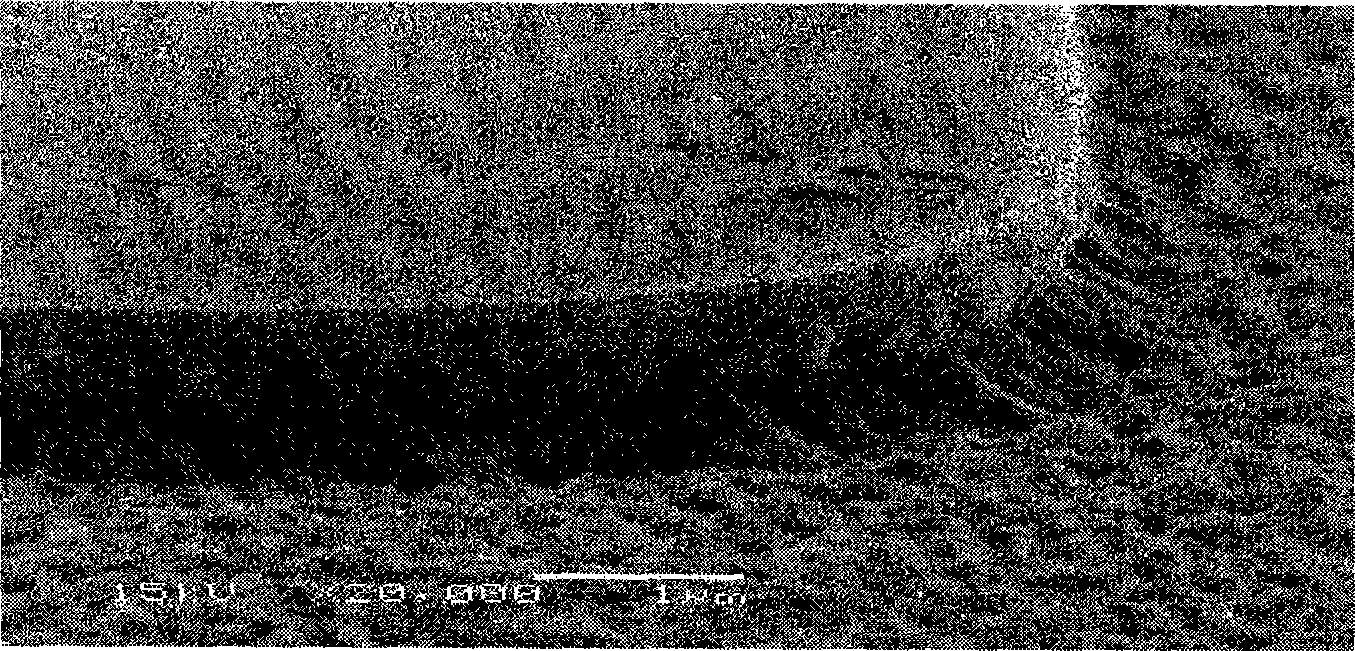
[0019] Example 1, such as figure 2 As shown in FIG. 1 , the side of the etched chip is inclined inward, showing an inverted mesa shape, and an inner chamfer is formed on the side.

[0020] Preparation method of LED chip:

[0021] (1) Using MOCVD epitaxy to grow GaN-based LED structure epitaxial wafers on sapphire substrates;

[0022] (2) Using a high-temperature annealing furnace, anneal the GaN epitaxial wafer at 760°C for 40 minutes in an N2 atmosphere to activate the P-type layer;

[0023] (3) Clean the surface of the GaN epitaxial wafer with acetone, ethanol, stripping solution, 10% hydrochloric acid, and deionized water.

[0024] (4) Photoetching the etched chip pattern on the GaN epitaxial wafer through uniform coating, baking, exposure, and development.

[0025] (5) Evaporate a 400nm Cr / Ni mask layer on the photoetched GaN epitaxial wafer by using an electron beam evaporation platform (E-600 machine of Taiwan Beiqiang Company).

[0026] (6) Remove the photoresist w...

Embodiment 2

[0029] Embodiment 2, the preparation method of LED chip:

[0030] (1) Using MOCVD epitaxy to grow GaN-based LED structure epitaxial wafers on sapphire substrates;

[0031] (2) Using a high-temperature annealing furnace, anneal the GaN epitaxial wafer at 760°C for 40 minutes in an N2 atmosphere to activate the P-type layer;

[0032] (3) Clean the surface of the GaN epitaxial wafer with acetone, ethanol, stripping solution, 20% hydrochloric acid, and deionized water.

[0033] (4) Photoetching the etched chip pattern on the GaN epitaxial wafer through uniform coating, baking, exposure, and development.

[0034] (5) Evaporate a 350nm Cr / Ni mask layer on the photoetched GaN epitaxial wafer by using an electron beam evaporation platform (E-600 machine of Taiwan Beiqiang Company).

[0035] (6) Remove the photoresist with acetone, ethanol, stripper, and deionized water.

[0036] (7), use ICP to etch the GaN to n-GaN layer, and make the chip side after etching inwardly inclined, in ...

Embodiment 3

[0037] Embodiment 3, the preparation method of LED chip:

[0038] (1) Using MOCVD epitaxy to grow GaN-based LED structure epitaxial wafers on sapphire substrates;

[0039] (2) Using a high-temperature annealing furnace, anneal the GaN epitaxial wafer at 760°C for 40 minutes in an N2 atmosphere to activate the P-type layer;

[0040] (3) Clean the surface of the GaN epitaxial wafer with acetone, ethanol, stripping solution, 30% hydrochloric acid, and deionized water.

[0041] (4) Photoetching the etched chip pattern on the GaN epitaxial wafer through uniform coating, baking, exposure, and development.

[0042] (5) Evaporate a 450nm Cr / Ni mask layer on the photoetched GaN epitaxial wafer by using an electron beam evaporation station.

[0043] (6) Remove the photoresist with acetone, ethanol, stripper, and deionized water.

[0044] (7), use ICP to etch the GaN to n-GaN layer, and make the chip side after etching tilt inward, in an inverted mesa shape, etching conditions: ICP po...


PUM


Abstract

The invention discloses an LED chip and a manufacturing method thereof, wherein the lateral surface of one ring around a chip after etching by an ICP is inwards inclined, and is in an inversed platform shape. The manufacturing method of the LED chip comprises the following steps: leading an epitaxial slice of a GaN base LED structure to grow on a sapphire substrate, leading the GaN epitaxial slice to anneal in high temperature under N2 atmosphere, cleanlily washing the surface of the GaN epitaxial slice by dissolvent, photo-etching graphs on the GaN epitaxial slice, evaporating and plating a Cr / Ni mask film layer on the GaN epitaxial slice, cleanlily removing photoresist by dissolvent, etching the epitaxial slice to a n-GaN layer by the ICP, and leading the lateral surface of the chip after etching to inwards incline to be in an inwards inversed platform shape, wherein the ICP etching condition is that ICP power is 1500W-2000W, RF power is 20W-40W, cavity pressure is 40-80mTorr, and etching gas flow ratio is that Cl2:Cl3=3-6:1.

Description

technical field [0001] The invention belongs to the technical field of chip production and relates to a method for producing high-brightness LED chips. Background technique [0002] In order to improve the luminous intensity of LED lighting, it is necessary to improve the photoelectric conversion efficiency of LED. The photoelectric conversion efficiency of LED includes two parts: internal quantum efficiency and external quantum efficiency. Efficiency; external quantum efficiency refers to the total efficiency after the photons generated in the LED junction area are extracted from the LED. At present, the internal quantum efficiency of commercial LEDs is close to 100%, but the external quantum efficiency is only 3-30%, which is mainly due to the light Due to the low escape, therefore, the external quantum efficiency has become the main technical bottleneck of high-brightness LED chips. The factors that cause light escape include: the absorption of light by lattice defects a...

Claims


Application Information

Patent Timeline
Patent Type & Authority Applications(China)
IPC IPC(8): H01L33/00
Inventor 谢雪峰
Owner 深圳市方大国科光电技术有限公司
Why Eureka
Try Eureka