Method for making high brightness LED chip

An LED chip, high-brightness technology, applied in electrical components, circuits, semiconductor devices, etc., can solve problems such as limiting the external quantum efficiency of GaN-based light-emitting diodes, and achieve the effects of improving external quantum efficiency, low cost, and simple process

Inactive Publication Date: 2009-07-01
深圳市方大国科光电技术有限公司
View PDF0 Cites 14 Cited by
  • Summary
  • Abstract
  • Description
  • Claims
  • Application Information

AI Technical Summary

Problems solved by technology

For the latter, it is because the reflection coefficients of GaN and air are 2.5 and 1 respectively, so the critical angle at which the light generated in the InGaN-GaN active region can propagat...

Method used


Image

  • Method for making high brightness LED chip
  • Method for making high brightness LED chip

Examples


Embodiment 1

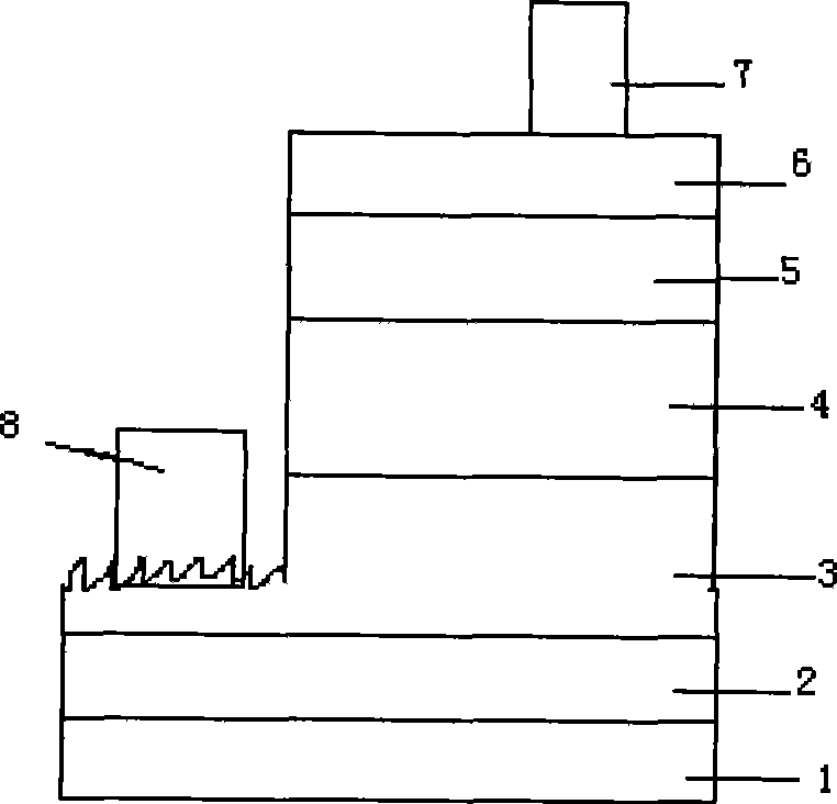
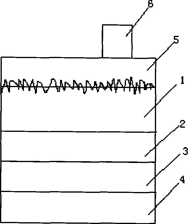
[0041] Example 1, such as figure 1 Shown is a front-mounted high-brightness LED chip, which includes a sapphire substrate 1, a GaN buffer layer 2, an n-type GaN layer 3, an InGaN / GaN multiple quantum well (MQws) active layer 4, a p-type GaN layer 5, from bottom to top. The p-type ohmic contact transparent electrode 6, the p-type ohmic contact metal electrode 7, and the n-type ohmic contact metal electrode 8.

[0042] The manufacturing method of the above-mentioned formally mounted high-brightness LED chip includes the following steps:

[0043] (1) On a sapphire substrate, use MOCVD to epitaxially grow a GaN-based LED structure epitaxial wafer;

[0044] (2) Use PECVD to deposit SiO on the epitaxial wafer 2 film;

[0045] (3) Use SiO 2 The thin film is used as a mask, and the N area pattern of the chip is photoetched on the epitaxial wafer by ICP dry etching technology;

[0046] (4) Use corrosive solution (40%N 4 HF: 40% HF: H 2 The volume ratio of O is 3: 1: 1) Cleaning the SiO th...

Embodiment 2

[0053] Embodiment 2, the manufacturing method of a high-brightness LED chip, including the following steps:

[0054] (1) On a sapphire substrate, use MOCVD to epitaxially grow a GaN-based LED structure epitaxial wafer;

[0055] (2) Use PECVD to deposit SiO on the epitaxial wafer 2 film;

[0056] (3) Use SiO 2 The thin film is used as a mask, and the N area pattern of the chip is photoetched on the epitaxial wafer by ICP dry etching technology;

[0057] (4) Use corrosive solution (40%N 4 HF: 40% HF: H 2 The volume ratio of O is 3: 1: 1) Cleaning the SiO that is not protected by photoresist 2 ;

[0058] (5) Clean the photoresist with stripping liquid;

[0059] (6) Use ICP to etch the N-side steps and the scribe lanes of the chip size to expose the n-GaN mesa;

[0060] (7) Use electron beam evaporation equipment to deposit Ti film on the epitaxial surface. The thickness of the Ti film is 300nm. Soak the epitaxial wafer in 30% KOH solution. At room temperature, use ordinary mercury lamp...

Embodiment 3

[0063] Embodiment 3, the manufacturing method of the high-brightness LED chip, including the following steps:

[0064] (1) On a sapphire substrate, use MOCVD to epitaxially grow a GaN-based LED structure epitaxial wafer;

[0065] (2) Use PECVD to deposit SiO on the epitaxial wafer 2 film;

[0066] (3) Use SiO 2 The thin film is used as a mask, and the N area pattern of the chip is photoetched on the epitaxial wafer by ICP dry etching technology;

[0067] (4) Use corrosive solution (40%N 4 HF: 40% HF: H 2 The volume ratio of O is 3: 1: 1) Cleaning the SiO that is not protected by photoresist 2 ;

[0068] (5) Clean the photoresist with stripping liquid;

[0069] (6) Use ICP to etch the N-side steps and the scribe lanes of the chip size to expose the n-GaN mesa;

[0070] (7) Use electron beam evaporation equipment to deposit Ti film on the epitaxial surface. The thickness of the Ti film is 280nm. Soak the epitaxial wafer in 5% hydrochloric acid solution at room temperature. Use ordin...


PUM

PropertyMeasurementUnit
Thicknessaaaaaaaaaa
Thicknessaaaaaaaaaa
Thicknessaaaaaaaaaa

Abstract

The invention discloses a high-brightness LED chip fabrication method, which comprises the following steps: generating an epitaxial wafer on a sapphire substrate; depositing a SiO2 film on the epitaxial wafer; etching an N-region patter on the chip by photolithography using the SiO2 film as the mask; cleaning the SiO2 not protected by the photoresist using a corrosive solution; cleaning with a photoresist removing solution to remove the photoresist; etching N steps and a track with the size of the chip to expose the n-GaN mesa; roughening the N-GAN surface by light-assisting wet etching; depositing an ITO film on the epitaxial wafer surface by evaporating; and evaporating a Cr/Ni/Au P-N electrode. The method can improve the external quantum efficiency of the LED device by increasing the probability of light refraction from the n-GaN to the air. The method can be used for fabricating normal LED chip and vertical LED chip, and has the advantages of simple process and low cost. The method suits industrial production and can greatly improve the external quantum efficiency.

Description

Technical field [0001] The invention belongs to the technical field of semiconductor lighting and relates to a method for manufacturing LED chips. Background technique [0002] The light output efficiency of LED chips lies in the external quantum efficiency and internal quantum efficiency. The external quantum efficiency is equal to the product of the internal quantum efficiency and the escape rate of light. Currently, the internal quantum efficiency of commercial LEDs is close to 100%, but the external quantum efficiency is only There are 3-30%, which is mainly caused by the low escape of light. Therefore, the external quantum efficiency has become the main technical bottleneck of high-brightness LED chips. The factors that cause light to escape include: the absorption of light by lattice defects, the absorption of light by the substrate, the loss of each interface due to total reflection in the process of light emission, and so on. For the latter, because the reflection coeffic...

Claims


Application Information

Patent Timeline
IPC IPC(8): H01L33/00
Inventor 欧阳红英
Owner 深圳市方大国科光电技术有限公司
Why Eureka
Try Eureka