

Nitride distributed Bragg reflector and production process thereof
A Bragg mirror, nitride technology, applied in semiconductor/solid-state device manufacturing, lasers, optical resonator structures, etc. Appearance, high quality effect
- Summary
- Abstract
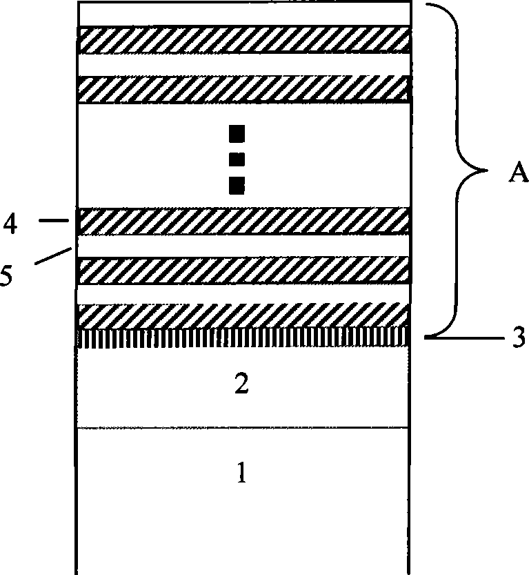
- Description
- Claims
- Application Information
AI Technical Summary
Problems solved by technology
Method used
Image

Examples
Embodiment 1
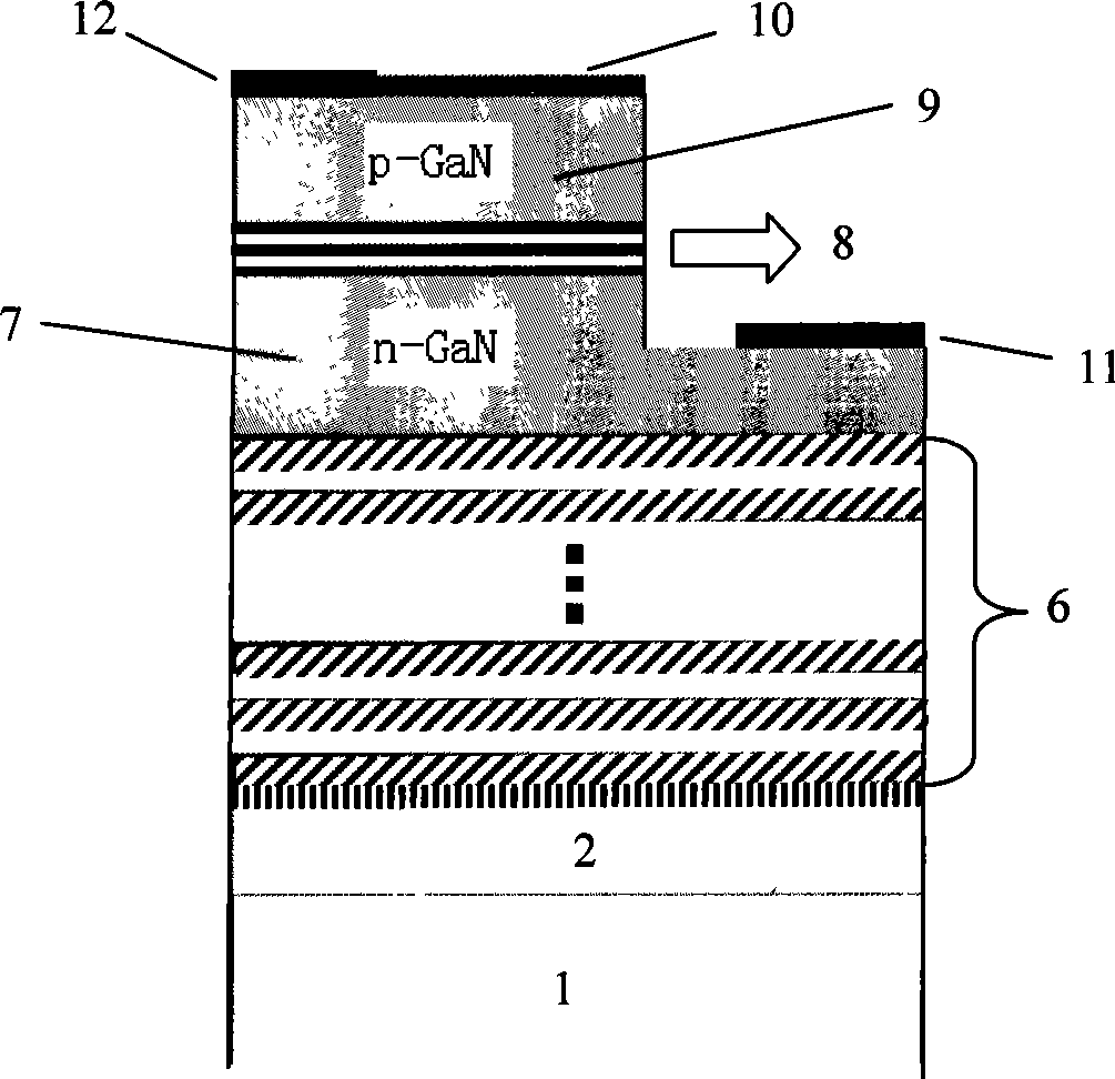
[0014] Embodiment 1: The corresponding structural diagram of MCLED is as follows image 3As shown, the GaN buffer layer 2 is deposited on the sapphire C-plane substrate 1 by MOCVD, and then the bottom nitride DBR structure 6 is deposited, and then a multilayer structure with a total thickness several times the wavelength (3 times in the figure) is grown ( It includes at least three parts including n-GaN7, InGaN / GaN multiple quantum well (MQWs) active layer 8 and p-GaN 9 from bottom to top), and then prepares the top reflector 10. The reflector can be metal reflective film such as Ag or Al or DBR. The n-type electrode 11 and the p-type electrode 12 can be formed on the n-GaN 7 and the p-GaN 9 shown in the figure respectively by photolithography, coupled plasma etching (ICP) and sputtering processes.
Embodiment 2
[0015] Embodiment 2: The corresponding structural diagram of VCSEL is as follows Figure 4 , using MOCVD to deposit a GaN buffer layer 2 on a sapphire C-plane substrate 1, then deposit a bottom nitride DBR structure 13, and re-grow a multilayer structure with a total thickness several times the wavelength (3 times in the figure) (from bottom to top in order Including n-GaN 14, InGaN / GaN multi-quantum well (MQWs) active layer 15 and p-GaN 16 etc. at least three parts), finally depositing top DBR structure 17. Dielectric film or nitride DBR can be selected according to needs. What is different from MCLED is that the position of the quantum well active layer in the VCSEL should be at the peak or trough position of the standing wave formed in the microcavity 18 (that is, the position of the maximum light field intensity in the cavity), and the reflectivity of the upper and lower mirrors should be large enough To meet the laser emission conditions.
PUM
| Property | Measurement | Unit |
|---|---|---|
| thickness | aaaaa | aaaaa |
| thickness | aaaaa | aaaaa |
| thickness | aaaaa | aaaaa |
Abstract
Description
Claims
Application Information