Display touch screen structure and method for producing the same
A manufacturing method and touch screen technology, which can be applied to instruments, ion implantation plating, coating, etc., can solve the problems of complex manufacturing process, high cost and low yield, and achieve simplified manufacturing process, reduced production cost and high yield. improved effect
- Summary
- Abstract
- Description
- Claims
- Application Information
AI Technical Summary
Problems solved by technology
Method used
Image

Examples
Embodiment Construction
[0012] In order to make the object, technical solution and advantages of the present invention more clear, the present invention will be further described in detail below in conjunction with the examples. It should be understood that the specific embodiments described here are only used to explain the present invention, not to limit the present invention.
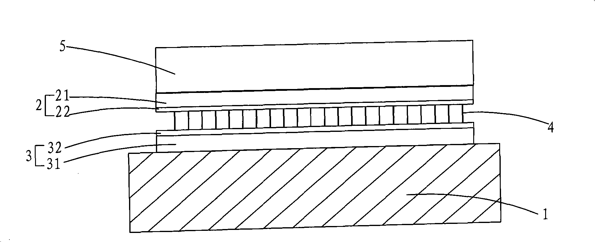
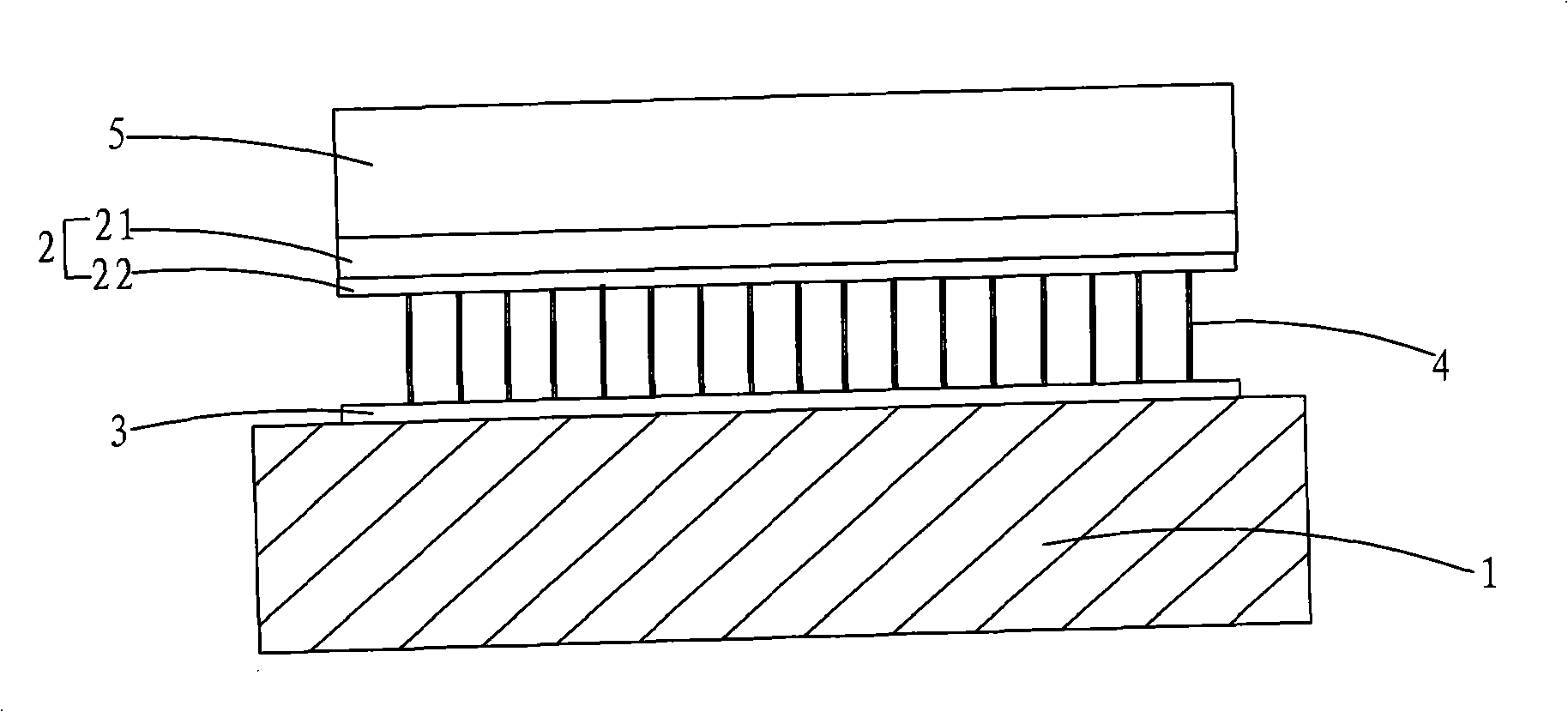
[0013] Compared with the prior art, the present invention provides a display touch screen structure with simple manufacturing process, improved product yield and reduced production cost, while ensuring that the strength of chemically strengthened glass does not change. Therefore, the embodiment of the present invention The conductive layer under the touch screen structure of the display is composed of an ITO film directly fabricated on the surface of the base chemically strengthened glass.
[0014] Specifically, figure 2 A display touch screen structure according to an embodiment of the present invention is shown, includi...
PUM
 Abstract
Description
Claims
Application Information
 - Generate Ideas
- Intellectual Property
- Life Sciences
- Materials
- Tech Scout
- Unparalleled Data Quality
- Higher Quality Content
- 60% Fewer Hallucinations
Browse by: Latest US Patents, China's latest patents, Technical Efficacy Thesaurus, Application Domain, Technology Topic, Popular Technical Reports.
© 2025 PatSnap. All rights reserved.Legal|Privacy policy|Modern Slavery Act Transparency Statement|Sitemap|About US| Contact US: help@patsnap.com