

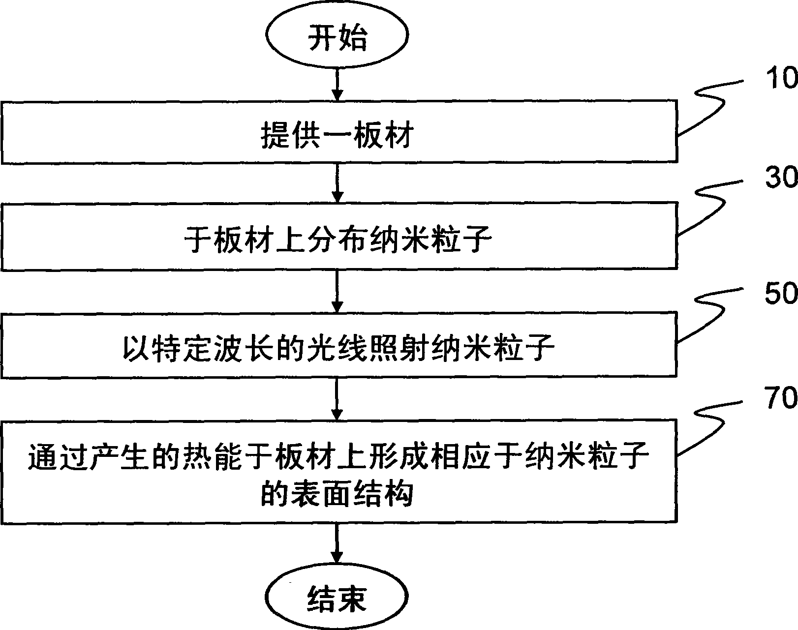
Method for manufacturing application substrate through photo-thermal effect
A photothermal effect and substrate technology, which is applied in printed circuit manufacturing, nanostructure manufacturing, electrical components, etc., can solve the problems of high cost, inability to produce large areas and large quantities, and complex processes, and achieve low cost, easy large area and large quantities. The effect of making and the overall process is simple
- Summary
- Abstract
- Description
- Claims
- Application Information
AI Technical Summary
Problems solved by technology
Method used
Image

Examples
example 1
[0095] Taking gold nanoparticles as an example, gold nanoparticles with a particle diameter of about 20 nm are fixed on a transparent substrate, and then placed on the surface of a polymer material plate. The gold nanoparticles will contact the surface of the plate. A green laser with a wavelength of 532nm is irradiated on the gold nanoparticles through the transparent substrate for about 15 seconds (the irradiation time is related to the material of the nanoparticles, the size of the nanoparticles, the concentration of the nanoparticles, the type of laser, the intensity of the laser, etc.) to excite the gold nanoparticles on the plate. of gold nanoparticles. At this time, the gold nanoparticles can generate heat energy up to about 200° C. within 15 seconds of the green laser irradiation. After the green laser irradiation is completed, the transparent substrate and gold nanoparticles on the plate are removed to obtain an application substrate with fine holes. Here, using an ...
example 2
[0099] A green laser with a wavelength of 532nm and a power of 100mW (milliwatts) is used to irradiate the gold nanoparticles placed on the plate 1 through the transparent substrate for about 10 minutes (irradiation time depends on the material of the nanoparticles, the size of the nanoparticles, the concentration of the nanoparticles, Laser type, laser intensity and other factors), and after the irradiation is completed, the transparent substrate and gold nanoparticles are removed to obtain the application substrate 1 . Here, using an atomic force microscope to observe the plate with gold nanoparticles before the green laser irradiation and the applied substrate 1 obtained after the laser irradiation, the following can be observed respectively: Figure 11A and Figure 11B Surface state shown.
example 3
[0101]A green laser with a wavelength of 514.5nm and a power of 1W (watts) was used to irradiate the gold nanoparticles on the plate 2 through the transparent substrate for about 20 minutes, and after the irradiation was completed, the transparent substrate and the gold nanoparticles were removed to obtain the application substrate 2 . Here, using an atomic force microscope to observe the plate with gold nanoparticles before irradiating the green laser and the applied substrate 2 obtained after the laser irradiating, the following can be observed respectively: Figure 12A and Figure 12B Surface state shown.
PUM
| Property | Measurement | Unit |
|---|---|---|
| particle diameter | aaaaa | aaaaa |
Abstract
Description
Claims
Application Information