Plane-structure InGaAs array infrared detector

An infrared detector and a planar structure technology, applied in the field of photodetectors, can solve problems such as the difficulty in defining the photosensitive surface, limiting the performance of InGaAs detectors, and large leakage currents, so as to suppress the expansion phenomenon and reduce the expansion phenomenon of the photosensitive surface , the effect of suppressing crosstalk

Active Publication Date: 2009-09-09
SHANGHAI INST OF TECHNICAL PHYSICS - CHINESE ACAD OF SCI
View PDF0 Cites 24 Cited by
  • Summary
  • Abstract
  • Description
  • Claims
  • Application Information

AI Technical Summary

Problems solved by technology

But it also has some unavoidable disadvantages: the expansion of the photosensitive surface makes it difficult to define the photosensitive surface, and the crosstalk between adjacent photosensitive surfaces is large, etc., which limit the improvement of the performance of InGaAs detectors.
At present, the general method is to use small diffusion holes to control the expansion of the photosensitive surface, use ring electrodes to define the photosensitive surface, and introduce guard rings to reduce device crosstalk. However, these methods are generally used alone and cannot fundamentally To solve the shortcomings of planar devices
In addition, for the extended-wavelength InGaAs array device with planar structure, due to the lattice mismatch of materials, there is a large leakage current between the P electrodes on the adjacent photosensitive surface, and the existing planar structure cannot solve this problem.

Method used


Image

  • Plane-structure InGaAs array infrared detector
  • Plane-structure InGaAs array infrared detector
  • Plane-structure InGaAs array infrared detector

Examples


Embodiment Construction

[0012] The specific embodiments of the present invention will be described in further detail below in conjunction with the accompanying drawings and examples:

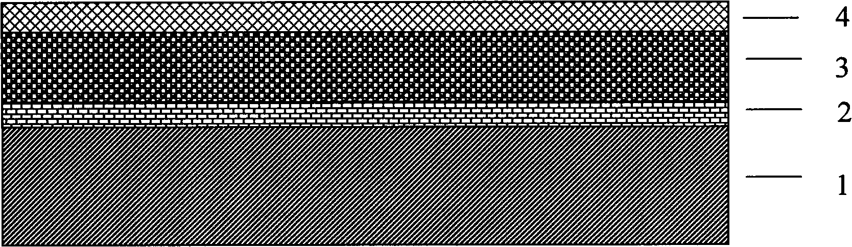
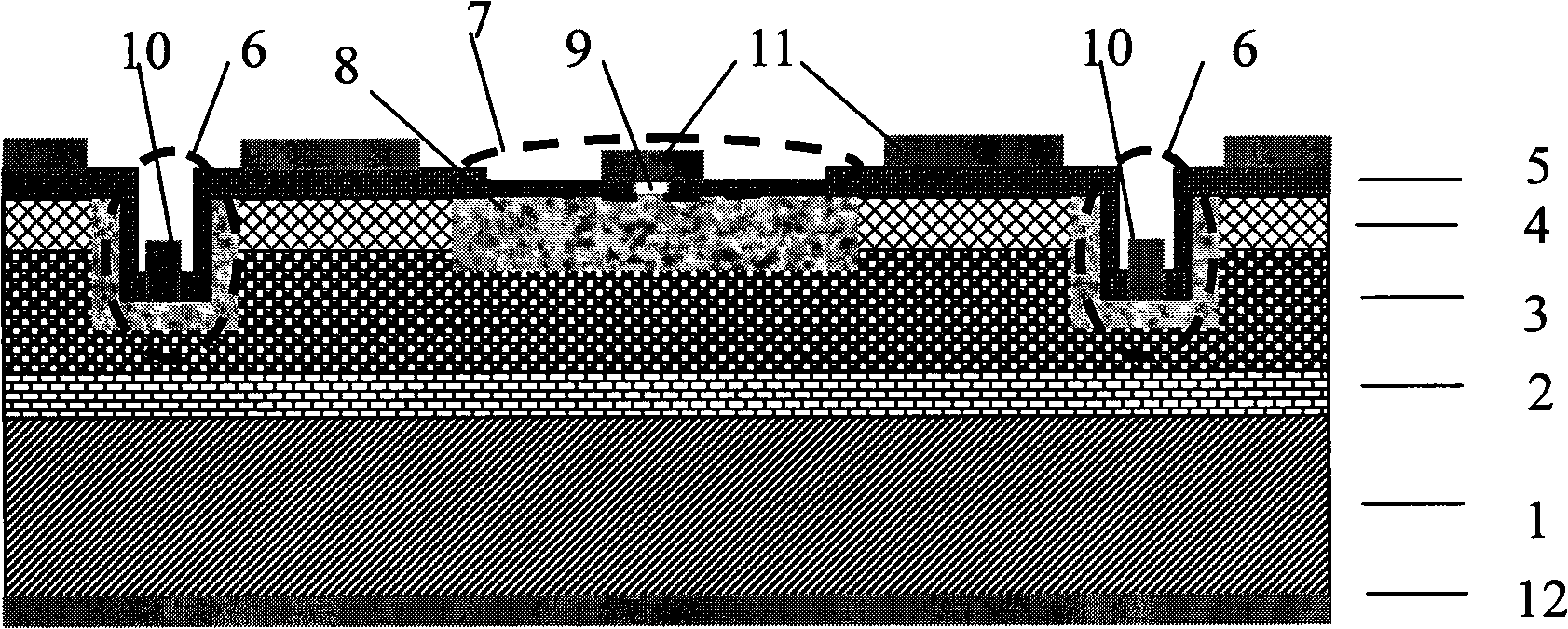
[0013] See figure 1 , the epitaxial wafer used in this embodiment is MOCVD technology with a thickness of 600 μm and a carrier concentration of 3 × 10 18 cm -3 N-type InP layers 2 with a thickness of 1 μm are sequentially grown on the N-InP substrate 1, and the carrier concentration is 2×10 18 cm -3 ; In thickness of 2.5 μm 0.53 Ga 0.47 As intrinsic absorption layer 3, carrier concentration 5×10 16 cm -3 ; N-type InP cap layer 4 with a thickness of 1 μm, carrier concentration 5 × 10 16 cm -3 .

[0014] The device preparation process of this embodiment is as follows:

[0015] 1. Use chloroform, ether, acetone, and ethanol to ultrasonically clean the epitaxial wafer in sequence for more than 2 minutes, and then blow dry with nitrogen;

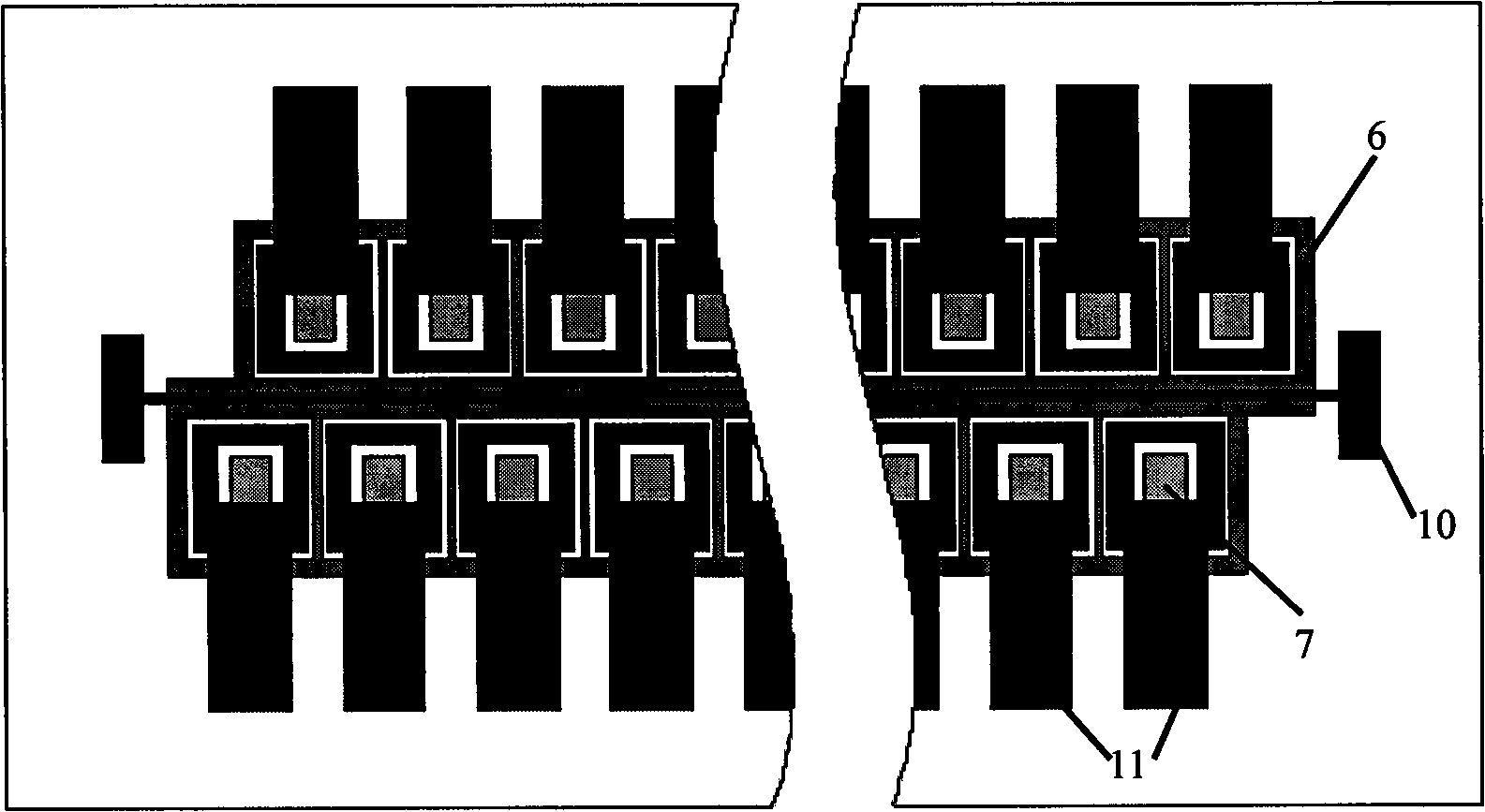
[0016] 2. Growth of SiO 2 Diffusion mask 5;

[0017] 3. Preparation of S...


PUM


Abstract

The invention discloses a novel plane-structure InGaAs array infrared detector. The structural design of the infrared detector is as follows: a shallow isolation groove is formed around an array photosensitive surface on an NIN-type epitaxial wafer by etching; a PN junction area of the photosensitive surface is formed by closed tube diffusion, and a guard ring integrated with the shallow isolation groove is formed; and guard ring electrodes and annular covering electrodes are formed by thickening Cr / Au. The novel plane-structure InGaAs array infrared detector has the advantages that the shallow isolation groove and the guard ring with the integrated design can effectively inhibit cross talk between adjacent photosensitive surfaces of an array device and enlargement of the photosensitive surfaces, and the enlargement of the photosensitive surfaces can be further inhibited and the photosensitive surfaces can be accurately defined if the infrared detector is aided with small diffusion holes and the annular covering electrodes. In the plane extension wavelength InGaAs array device, the shallow isolation groove can also help effectively inhibit drain current between P electrodes of adjacent photosensitive surfaces caused by lattice mismatching of materials.

Description

technical field [0001] The photodetector technology involved in the present invention specifically refers to a planar structure indium gallium arsenide array infrared detector. Background technique [0002] At present, PIN InGaAs detectors are mainly divided into two types: planar type and mesa type. The mesa-type InGaAs detector is to etch the P-InP / InGaAs in the epitaxial material into a mesa, which fundamentally isolates the adjacent photosensitive surfaces. The detector of this structure has the advantages of simple preparation process and adjacent photosensitive surfaces. It has the advantages of low crosstalk and easy definition of the photosensitive surface, but the exposed side of the mesa detector brings great difficulties to the passivation of the device, which will reduce the reliability of the device and increase the noise. Limiting the improvement of device detection rate. As the mainstream structure of indium gallium arsenide detectors, planar indium gallium ...

Claims


Application Information

Patent Timeline
Patent Type & Authority Applications(China)
IPC IPC(8): H01L27/144H01L31/109H01L31/02
Inventor 李永富龚海梅李雪唐恒敬张可锋李淘宁锦华张燕朱耀明姜佩璐
Owner SHANGHAI INST OF TECHNICAL PHYSICS - CHINESE ACAD OF SCI
Why Eureka
Try Eureka