An anti-SEU storage cell circuit in an anti-radiation hardening FPGA chip

A storage unit circuit, anti-radiation hardening technology, applied in information storage, static memory, digital memory information and other directions, can solve the problems of inability to meet the needs of anti-radiation FPGA chips, high resistance noise and power consumption, and less use of circuits. Enhance the ability to resist single-event flipping, improve anti-single-event flipping ability, and increase the effect of current pulse time

Inactive Publication Date: 2009-10-07
BEIJING MXTRONICS CORP +1
View PDF1 Cites 24 Cited by
  • Summary
  • Abstract
  • Description
  • Claims
  • Application Information

AI Technical Summary

Problems solved by technology

Therefore, the required PMOS tube has a large width-to-length ratio, which is difficult to realize in FPGA chips, and the resistance noise and power consumption are relatively large, so it cannot meet the needs of radiation-resistant FPGA chips in space environments.
Figure 4 In, another alternative structure is proposed, using the first inductance 143 and the second inductance 144 to replace figure 1 In the implementation of the second resistor 15 and the first resistor 13, the inductance is enhanced by limiting the transient current pulse caused by the single event flipping Figure 4 The ability of anti-single event reversal of the circuit shown, but because it is relatively difficult to make inductors by using CMOS technology, so this kind of circuit is rarely used in engineering

Method used


Image

  • An anti-SEU storage cell circuit in an anti-radiation hardening FPGA chip
  • An anti-SEU storage cell circuit in an anti-radiation hardening FPGA chip
  • An anti-SEU storage cell circuit in an anti-radiation hardening FPGA chip

Examples


Embodiment Construction

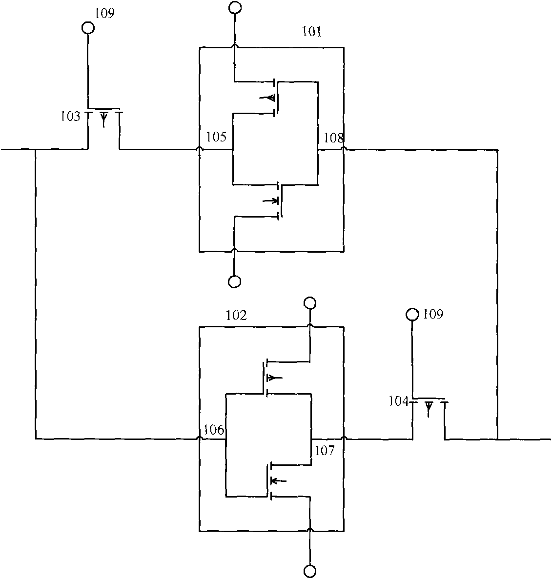
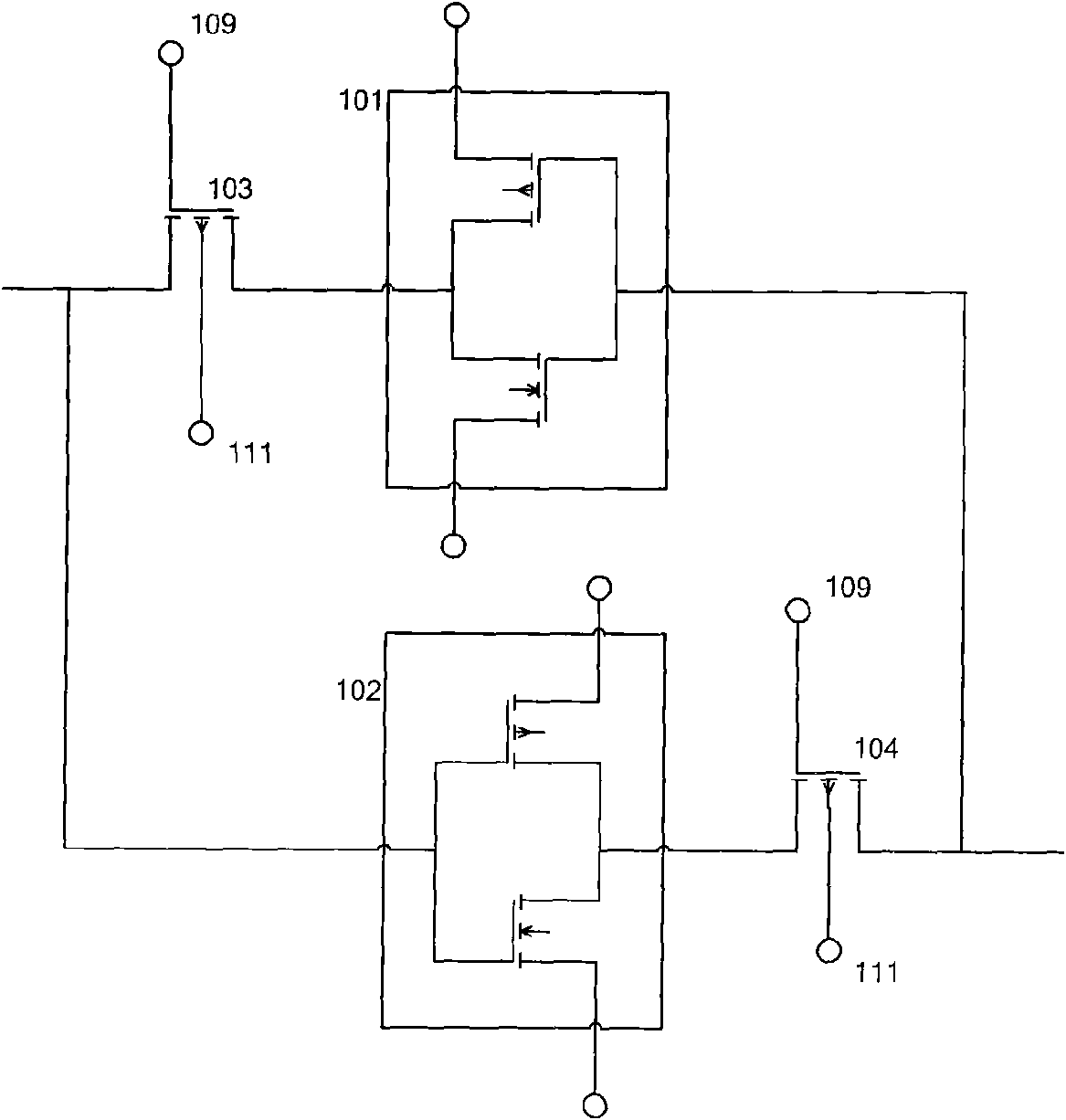
[0026] Such as Figure 5 As shown, it is a design schematic diagram of the storage circuit against single event upset in the FPGA chip of the present invention. Figure 5 The circuit diagram shown is an improved radiation-hardened CMOS SRAM memory cell, including a first inverter 501, a second inverter 502, a first transistor 503, and a second transistor 504, and the source terminal and drain terminal of the first transistor 503 are One end of the transistor is connected to the output terminal 505 of the first inverter 501, and the other end is connected to the input terminal 506 of the second inverter 502; one end of the source terminal and the drain terminal of the second transistor 504 is connected to the first inverter The input terminal 508 of 501, the other end is connected to the output terminal 507 of the second inverter 502; The input terminal 508 of the first inverter 501 and the input terminal 506 of the second inverter 502 are used as the data input and output of t...


PUM


Abstract

The anti-SEU storage cell circuit in an anti-radiation hardening FPGA chip includes two inverters and two transistors. The two inverters are cross connected and realize the adjustment to the resistance values at the source terminals and drain terminals of the two transistors through controlling the grid voltage and substrate potential of the two transistors. The resistance values are not greater than 50 omega or not smaller than 1,000 omega. With respect to inverter design, a resistor is added to the existing circuit consisting of PMOS tube and NMOS tube. The resistor is connected between the drain terminals of PMOS transistor and NMOS transistor. Through adding a resistor into the inverter, the present invention realizes anti-SEU (single event upset) of the storage cell. Moreover, the storage circuit of the present invention has the following advantages: small noise, low power consumption, small area occupied, and easy realization of layout and process in the design of anti-radiation hardening FPGA chip.

Description

technical field [0001] The invention relates to a memory unit circuit, in particular to a memory unit circuit realized in an FPGA chip and capable of effectively preventing single event reversal effect. Background technique [0002] A field programmable logic device (FPGA) has become a well-known integrated circuit (IC) that can be programmed by a user to implement a specific logic function. There are many different types of programmable logic devices, for example, programmable logic arrays (PLAs), complex programmable logic devices (CPLDs). A type of programmable logic device called a field-programmable logic array (FPGA) is popular with designers because of its advantages in storage capacity, flexibility, development time, and cost. A typical FPGA includes an array of programmable logic blocks (CLBs) and a circle of programmable input / output blocks (IOBs) surrounding the CLBs. CLBs and IOBs are connected by programmable interconnect resources. A typical programming meth...

Claims


Application Information

Patent Timeline
Patent Type & Authority Applications(China)
IPC IPC(8): G11C11/412
Inventor 陈雷文治平王雷王慜孙华波李学武刘增荣周涛张帆尚祖宾
Owner BEIJING MXTRONICS CORP
Why Eureka
Try Eureka