
Film silicon photovoltaic device and manufacturing method, back electrode and photovoltaic component thereof

A technology of photovoltaic devices and thin-film silicon, which is applied in photovoltaic power generation, semiconductor devices, and final product manufacturing. Achieve the effects of avoiding TCO deposition process, suppressing shunt and instability, and good photoelectric conversion efficiency

Active Publication Date: 2009-10-14
GS SOLAR FU JIAN COMPANY +1
View PDF0 Cites 7 Cited by
  • Summary
  • Abstract
  • Description
  • Claims
  • Application Information

AI Technical Summary

Problems solved by technology

[0006] However, there are serious problems with the combination of Zn0 / Ag
First, when the silicon layer of a thin-film silicon cell is thin, a sufficiently thick silver film required for low resistance can lead to significant shunts in many areas of the cell, reducing the energy conversion rate and reducing the efficiency of the photovoltaic module. Low yield
Shunt shorting tends to get worse over time and is especially problematic in the production of large area stencils
Second, the use of a thicker silver film as the back electrode significantly reduces the stability of the photovoltaic template, because silver atoms are activated by temperature under the influence of an electric field to migrate, allowing silver to diffuse into the silicon film along structural defects
Third, the instability of the silver film when exposed to moisture-containing air causes its light reflectance to decrease significantly after several months or more, which leads to the loss of power generation capacity and life of the photovoltaic template
Fourth, since silver is a precious metal, the use of thicker silver films results in higher production costs
This method can obtain uniform and reproducible large-area ZnO:Al thin films by using ceramic targets, but its disadvantages are: high equipment cost, complex target fabrication, low deposition rate (i.e., low throughput), and the substrate should be Heating to a higher temperature (for example, between 100°C and 200°C) makes the magnetron sputtering equipment capable of high-speed operation and its operation very complicated
However, especially during heat treatment at moderate temperatures (such as 130°C-200°C), the silver and aluminum films are easily mixed with each other due to diffusion.
Therefore, the light reflectance of the silver film tends to be reduced
Furthermore, as mentioned above, the deposition of ZnO is a very difficult low-throughput process

Method used


Image

  • Film silicon photovoltaic device and manufacturing method, back electrode and photovoltaic component thereof
  • Film silicon photovoltaic device and manufacturing method, back electrode and photovoltaic component thereof

Examples


Embodiment Construction

[0035] Preferred embodiments of the present invention will be described in detail below with reference to the accompanying drawings, in which like reference numerals denote like elements throughout. It should be understood that the embodiments described herein are illustrative only and should not be construed as limiting the scope of the present invention.

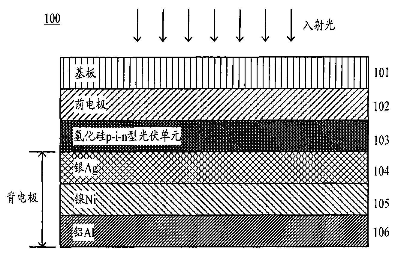
[0036] The proposal of the back electrode according to the invention is based on the following important facts. Silver and nickel are matching metal materials, and the optical and / or conductive properties of the back electrode will not be significantly affected by the diffusion of silver atoms and nickel atoms between the silver film and the nickel film. In contrast, in conventional back electrodes, severe interdiffusion occurs between silver and aluminum (Ag / Al) thin films, resulting in poor optoelectronic performance of the back electrodes. In addition, nickel has good electrical conductivity and chemical stability, as ...


PUM


Abstract

The invention discloses a film silicon photovoltaic device and a manufacturing method, a back electrode and a photovoltaic component thereof. The film silicon photovoltaic device has a layered structure sequentially comprising a base plate, a transparent conductive front electrode, one or a plurality of p-i-n type photovoltaic cells and a back electrode, wherein each p-i-n type photovoltaic cell consists of a p type semiconductor film, an intrinsic i type semiconductor film and an n type semiconductor film which are based on hydrogenated silicon; the back electrode contains a silver film, a nickel film and an aluminum film which are sequentially overlapped, the silver film is positioned on one side of the back electrode, which is adjacent to the p-i-n type photovoltaic cell, and the nickel film is made of nickel or a nickel alloy containing higher than 60 percent of nickel. The full metal type back electrode made of silver, nickel and aluminum has the advantages of having high reflectivity, good electrical conductivity and strong stability, being not short-circuited easily, being convenient for producing large-area photovoltaic templates in low cost, and the like.

Description

technical field [0001] The present invention relates to the field of solar photovoltaic devices, and in particular to a thin-film silicon photovoltaic device and a manufacturing method thereof, a back electrode used for the thin-film silicon photovoltaic device, and a photovoltaic module composed of a plurality of thin-film silicon photovoltaic devices. Background technique [0002] Solar energy is a renewable energy and a clean energy that does not produce any environmental pollution. Solar photovoltaic (photovoltaic) cells are one of the hot research areas in recent years, and have formed a high-profile emerging industry. Solar cells are mainly manufactured on the basis of semiconductor materials, and their working principle is to use photoelectric materials to absorb light energy and generate photoelectric conversion reactions of photoelectrons. Different materials can be used for solar cells, including crystalline silicon, III-V compounds such as gallium arsenide, cryst...

Claims


Application Information

Patent Timeline
Patent Type & Authority Applications(China)
IPC IPC(8): H01L31/075H01L31/052H01L31/0224H01L31/18H01L31/054
CPCY02E10/52Y02E10/548Y02P70/50
Inventor 李沅民杨与胜
Owner GS SOLAR FU JIAN COMPANY
Learn More