Silica-based germanium electrical injection laser and production method thereof

A laser and silicon-based technology, applied in the direction of lasers, laser components, semiconductor lasers, etc., can solve problems such as the lack of light emission

Inactive Publication Date: 2009-10-14
UNIV OF ELECTRONIC SCI & TECH OF CHINA
View PDF0 Cites 9 Cited by
  • Summary
  • Abstract
  • Description
  • Claims
  • Application Information

AI Technical Summary

Problems solved by technology

In 2000, the Pavesi group in Italy realized the optical gain under strong optical pumping conditions for the first time in the nanocrystal system embedded in silicon dioxide, and the gain coefficient was about 100cm -1 (British Nature, 2000 V408 (6811): p440-444), in 2004, Dr. Chen Minzhang from the Cai Zhenshui group of Taiwan's "Academia Sinica" reported the realization of the first silicon-based electric injection lasing (U.S. Appl.Phys.Lett, 2004, v 84, n 12, p2163-2165), in 2004, Holland Polman group realized silicon oxide erbium-doped ring resonator optical pump lasing (US Appl. Phys. Lett 84 p1037-1039 (2004)), in 2005, Brown University JimmyXu's group reported optical pumping based on silicon-based and other electronic doping (Nature materials, UK, 2005, V4(12): p887-891), but silicon-based and other electronic doping is a long-standing problem that has not been solved for many years. Even room temperature luminescence has not been realized until now (Applied Physics Letters V90, 081101 (2007) in the United States), and the possibility of further major breakthroughs in the short term is very slim

Method used


Image

  • Silica-based germanium electrical injection laser and production method thereof
  • Silica-based germanium electrical injection laser and production method thereof

Examples


Embodiment Construction

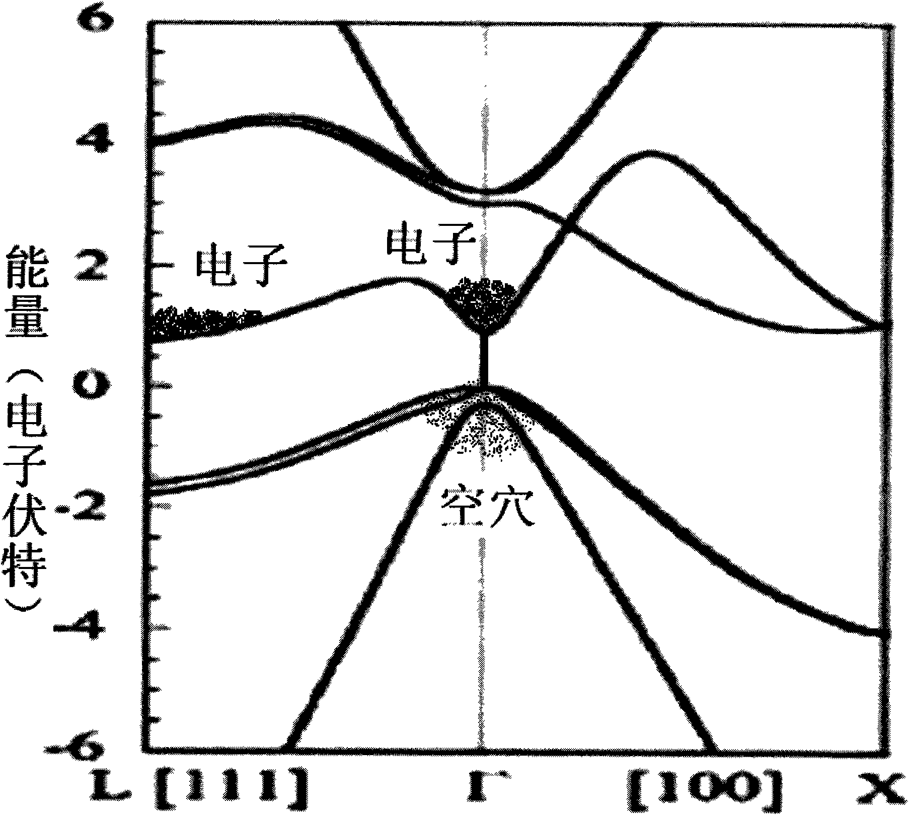
[0043] from figure 1 It can be seen from the energy band structure diagram of germanium that germanium is an indirect bandgap semiconductor material, the lowest conduction band valley is located at the L point ( direction) of the Brillouin zone, and the second lowest conduction band valley is located at the Brillouin zone center Г point ( k=0), there is the second lowest X point in the direction. The energy gap difference between the Г conduction band valley and the L conduction band valley is about 0.136eV (room temperature), and the X conduction band valley is about 0.18eV higher than the Г conduction band valley (room temperature). According to the Boltzmann distribution principle, at higher temperatures, in addition to the main electron concentration in the lowest L conduction band valley, there are also a relatively large number of electrons (not more than 5%) in the Γ conduction band valley.

[0044] However, even so, under normal circumstances, germanium-based materia...


PUM

PropertyMeasurementUnit
Doping concentrationaaaaaaaaaa

Abstract

The invention relates to a silica-based germanium electrical injection laser and a production method thereof. An active layer of the laser forms a p-i-n structure on the basis of an extension germanium-based single crystalline layer on a monocrystal line silicon. A first limiting layer is positioned at the upper part of the active layer, and a second limiting layer is positioned at the lower part of the active layer. Under the injection of large electric current, when the injected electric current is larger than or equal to a laser ejection threshold, the laser utilizes Auger effect and a laser resonant cavity to form positive feedback to adjust the electronic condensation proportion of a germanium L conduction band valley and a germanium inverse-L conduction band valley so as to realize the higher electronic condensation of the germanium inverse-L conduction band valley, therefore, the silica-based germanium electrical injection laser which realizes high efficiency and low working current density and is based on germanium direct bandgap near infrared (-1.55 microns) light emission is achieved.

Description

technical field [0001] The invention relates to a silicon-based electrical injection laser and a manufacturing method, in particular to a silicon-based germanium electrical injection laser and a manufacturing method based on germanium direct bandgap near-infrared (~1.55 μm) light emission. Background technique [0002] As we all know, silicon-based ultra-large-scale integration (ULSI) is the cornerstone of the information revolution. The computing speed of today's chips is getting faster and faster, and the speed of corresponding information transmission will also be faster and faster. Unfortunately, now relying on improving the operation speed of a single transistor or logic gate to increase the operation speed of the overall integrated circuit chip will reach the limit due to the limitation of physical effects; The speed is no longer the operation speed of a single transistor or logic gate, but more from the delay of signal transmission between transistors or / and logic ga...

Claims


Application Information

Patent Timeline
IPC IPC(8): H01S5/00H01S5/042H01S5/062H01S5/32H01L33/00H01L21/00
Inventor 张建国
Owner UNIV OF ELECTRONIC SCI & TECH OF CHINA
Why Eureka
Try Eureka