Integrated optoelectronic device based on sideband injection locking and used for generating high-frequency microwaves

An optoelectronic device, injection locking technology, applied in laser parts, lasers, electrical components and other directions, can solve the problems of large and complex system, poor stability, high cost, and achieve the effect of simple manufacturing process, low cost and high yield

Inactive Publication Date: 2009-10-28
TSINGHUA UNIV
View PDF0 Cites 16 Cited by
  • Summary
  • Abstract
  • Description
  • Claims
  • Application Information

AI Technical Summary

Problems solved by technology

As we all know, the systems built by discrete devices are often large and complex, with poor stability and relatively high cost.

Method used


Image

  • Integrated optoelectronic device based on sideband injection locking and used for generating high-frequency microwaves
  • Integrated optoelectronic device based on sideband injection locking and used for generating high-frequency microwaves
  • Integrated optoelectronic device based on sideband injection locking and used for generating high-frequency microwaves

Examples


Embodiment 1

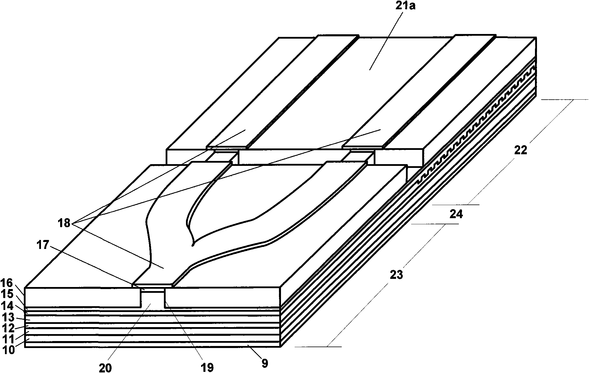
[0049] Example 1 figure 2 It is a Y-branch waveguide coupled photo-generated microwave integrated optoelectronic device that integrates two slave lasers. The operating wavelength is in the 1550nm band, and on the basis of using an external discrete tunable laser and an external modulator for injection, the InGaAsP / InP-based integrated optoelectronic device that generates high-frequency microwaves is locked by sideband injection.

[0050] This device integrates two DFB lasers 21a as slave lasers 22 and a Y-branch waveguide 23 on one chip.

[0051] First, the epitaxial materials of the device are as follows. By metal organic chemical vapor deposition (Metal Organic Chemical Vapor Deposition, MOCVD) method, first epitaxy on the n-type substrate 10 material, and then grow the n-type InP lower cladding layer 10 (thickness 200nm, doping concentration about 1×10 18 cm -2), 100nm thick undoped lattice-matched InGaAsP waveguide layer 11 (photoluminescence wavelength 1.2μm), straine...

Embodiment 2

[0054] Example 2 Figure 4 It is an MMI coupled photo-generated microwave integrated optoelectronic device that integrates two slave lasers. The operating wavelength is in the 1550nm band, and on the basis of using an external discrete tunable laser and an external modulator for injection, the InGaAsP / InP-based integrated optoelectronic device that generates high-frequency microwaves is locked by sideband injection.

[0055] This device integrates two DFB lasers 21a as slave lasers 22 and one MMI 25 on one chip.

[0056] First, the epitaxial materials of the device are as follows. Through the MOCVD method, first epitaxially grow the n-type InP lower cladding layer 10 (thickness 200nm, doping concentration about 1×10) on the n-type substrate 10 material 18 cm -2 ), 100nm thick undoped lattice-matched InGaAsP waveguide layer 11 (photoluminescence wavelength 1.2μm), strained InGaAsP multiple quantum wells 12 (photoluminescence wavelength 1.52μm, 7 quantum wells: well width 8nm...

Embodiment 3

[0059] Example 3 Image 6 It is a Y-branch waveguide coupled photo-generated microwave integrated optoelectronic device that integrates a master laser and two slave lasers. The operating wavelength is within the 1550nm band, and on the basis of direct modulation of the main laser, the InGaAsP / InP-based integrated optoelectronic device that uses sideband injection locking to generate high-frequency microwaves.

[0060] This device integrates two DFB lasers 21 a as slave lasers 22 , one DFB laser 21 b as master laser 26 and two Y-branch waveguides 23 on one chip.

[0061] First, the epitaxial materials of the device are as follows. Through the MOCVD method, first epitaxially grow the n-type InP lower cladding layer 10 (thickness 200nm, doping concentration about 1×10) on the n-type substrate 10 material 18 cm -2 ), 100nm thick undoped lattice-matched InGaAsP waveguide layer 11 (photoluminescence wavelength 1.2μm), strained InGaAsP multiple quantum wells 12 (photoluminescence ...


PUM

PropertyMeasurementUnit
lengthaaaaaaaaaa
lengthaaaaaaaaaa
lengthaaaaaaaaaa

Abstract

The invention provides an integrated optoelectronic device based on sideband injection locking and used for generating high-frequency microwaves, belonging to the technical field of optoelectronic device preparation of microwave optoelectronics field, particularly relating to an integrated optoelectronic device based on sideband injection locking and used for generating high-frequency microwaves. The integrated optoelectronic device integrates two slave lasers on the same substrate, sequentially extends a lower waveguide layer, a multi-quantum well active layer, a grating layer, an upper waveguide layer, an upper cladding layer and an Ohmic contact layer on the substrate, couples two slave lasers together by a Y branch waveguide or a multi-mode interferometer, thus realizing injection of modulation sideband of external main laser and carrying out injection locking; and heterodyne beat is conducted by the coupling output of the Y branch waveguide or the multi-mode interferometer, thus being capable of obtaining the high-frequency microwave. The integrated optoelectronic device can integrate a main laser and an electro-absorption modulator further and improve the integration further. The integrated optoelectronic device has novel structure, simple preparation process and excellent application prospect in the future field of high-speed communication.

Description

technical field [0001] The invention belongs to the technical field of optoelectronic device preparation in the field of microwave photonics, and in particular relates to an integrated optoelectronic device for generating high-frequency microwaves by using sideband injection locking. technical background [0002] The invention is an integrated optoelectronic device that uses sideband injection locking to generate high-frequency microwaves, and then generates high-frequency microwaves through optical heterodyning. Its application range is very wide, including wireless local area network, antenna remote control and so on. The following first briefly introduces the importance of high-frequency microwave or millimeter wave in wireless communication, and then introduces the application of optoelectronic technology in millimeter wave wireless communication. [0003] In recent years, with the continuous development of optical fiber networks and the Internet (Internet), voice, image...

Claims


Application Information

Patent Timeline
Patent Type & Authority Applications(China)
IPC IPC(8): G02F1/35H01S5/026H04B10/155
Inventor 孙长征黄缙熊兵罗毅
Owner TSINGHUA UNIV
Why Eureka
Try Eureka