Semiconductor device, p-type MOS transistor and manufacturing method thereof

A technology of MOS transistors and manufacturing methods, applied in the field of p-type MOS transistors and their manufacturing, and semiconductor devices, can solve the problems of NBTI effect enhancement, avalanche collision, and influence on the characteristics and reliability of semiconductor devices, and achieve the effect of reducing the impact

Active Publication Date: 2009-11-04
SEMICONDUCTOR MANUFACTURING INTERNATIONAL (BEIJING) CORP
View PDF1 Cites 16 Cited by
  • Summary
  • Abstract
  • Description
  • Claims
  • Application Information

AI Technical Summary

Problems solved by technology

[0008] However, in the above technical scheme, due to the use of hydrogen in the oxidation and annealing process, there will always be some Si-H bonds at the silicon-oxygen interface when silicon oxide is formed, which is difficult to completely remove. The key will enhance the NBTI effect and affect the performance of MOS transistors
[0009] Moreover, these Si-H bonds at the interface between the semiconductor substrate and the gate dielectric layer will bring another problem, that is, when a strong electric field exists, it is very easy to be bombarded by hot electrons and break, forming a large number of electron traps, which will seriously affect the semiconductor performance. Device characteristics and reliability, especially in high-voltage devices, that is, input and output devices, due to the strong electric field, these defects are more prone to the hot electron injection effect caused by avalanche impact ionization

Method used


Image

  • Semiconductor device, p-type MOS transistor and manufacturing method thereof
  • Semiconductor device, p-type MOS transistor and manufacturing method thereof
  • Semiconductor device, p-type MOS transistor and manufacturing method thereof

Examples


Embodiment Construction

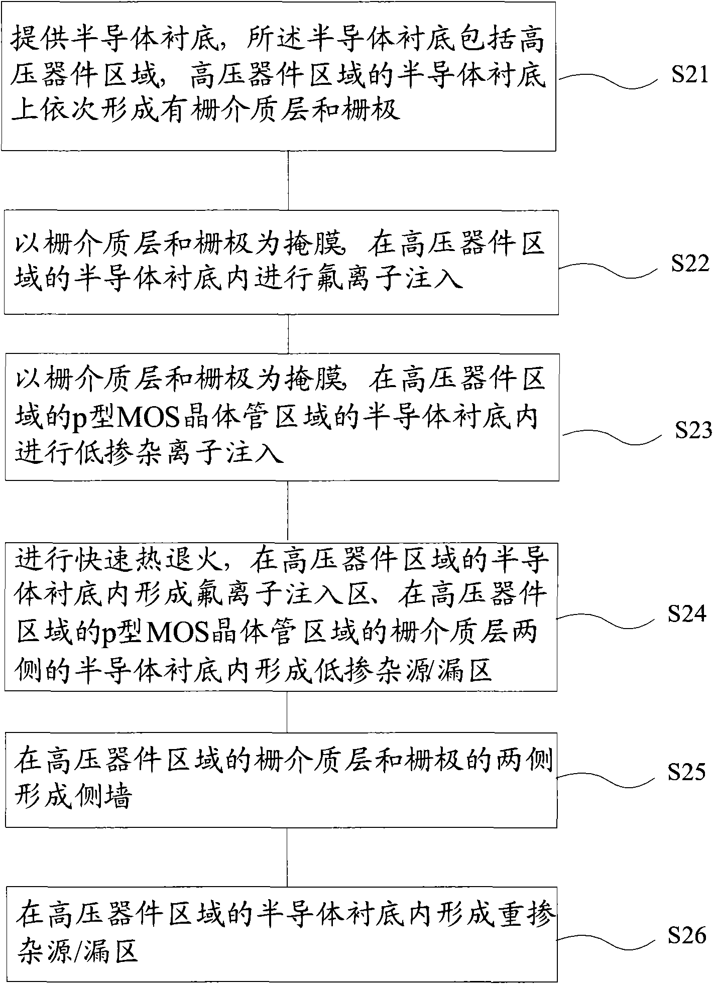
[0034] In the present invention, a fluorine ion implantation area is formed on the surface of the semiconductor substrate on the low-doped source / drain area of ​​the p-type MOS transistor area of ​​the high voltage device area, and the fluorine ion in the fluorine ion implantation area and the silicon in the semiconductor substrate form fluorine silicon Since the silicon-fluorine bond is stronger than the silicon-hydrogen bond, it prevents the formation of Si dangling bonds at high temperatures, thereby reducing the impact of the NBTI effect on the MOS transistor.

[0035] In the present invention, a fluorine ion implantation area is formed on the surface of the semiconductor substrate on the low-doped source / drain area of ​​the p-type MOS transistor area of ​​the high voltage device area, and the fluorine ion in the fluorine ion implantation area and the silicon in the semiconductor substrate form fluorine silicon The group is beneficial to reduce the trap charge and dislocation ...


PUM


Abstract

The invention relates to a semiconductor device, a p-type MOS transistor and a manufacturing method thereof. The method for manufacturing the semiconductor device comprises the following steps: providing a semiconductor substrate; taking a grid medium layer and a grid electrode as masks, and implanting fluorine ions into a semiconductor substrate in a high-voltage device region; taking the grid medium layer and the grid electrode as the masks, and implanting low doped ions into a semiconductor substrate in the p-type MOS transistor region of the high-voltage device region; performing quick thermal annealing; forming side walls on both sides of the grid medium layer and the grid electrode in the high-voltage device region; and forming a heavy doping source / drain region in the semiconductor substrate of the high-voltage device region. The invention also provides the semiconductor device, the p-type MOS transistor and the manufacturing method thereof. The invention is favorable for restricting the influence of the NBTI effect on the MOS transistor by forming a fluorine ion implantation region on a low doping source / drain region in the p-type MOS transistor region of the high-voltage device region, and simultaneously can reduce the hot carrier injection effect.

Description

Technical field [0001] The present invention relates to the field of semiconductor technology, in particular to semiconductor devices, p-type MOS transistors and manufacturing methods thereof. Background technique [0002] With the development of technology and the continuous shrinking of device size, p-type MOS transistors are becoming more and more serious due to the influence of negative temperature bias instability effect (NBTI). The NBTI effect has become a focal issue affecting device reliability. . The NBTI means that the threshold voltage of the p-type MOS transistor drifts under the action of stress at high temperature, so NBTI is an important reliability requirement. With the further development of the miniaturization of interconnections, the gate dielectric layer tends to become thinner, so that the NBTI effect needs to be further improved. [0003] At present, although the exact cause of NBTI has not been clarified, known experience shows that when the Si-H bond conce...

Claims


Application Information

Patent Timeline
Patent Type & Authority Applications(China)
IPC IPC(8): H01L21/8234H01L21/336H01L27/04H01L29/78H01L29/08
Inventor 赵猛王津洲
Owner SEMICONDUCTOR MANUFACTURING INTERNATIONAL (BEIJING) CORP
Why Eureka
Try Eureka