Dual bootstrap and voltage compensation technology-based A/D converter sampling switch

A technology of voltage compensation and sampling switch, which is applied in the field of microelectronics and solid-state electronics, and can solve problems such as limiting the range of input signals, not being able to completely replicate the M1 tube, and lowering the upper limit of switching speed

Active Publication Date: 2009-11-11
INST OF ELECTRONICS CHINESE ACAD OF SCI
View PDF0 Cites 26 Cited by
  • Summary
  • Abstract
  • Description
  • Claims
  • Application Information

AI Technical Summary

Problems solved by technology

[0008] Two problems can be found from the formula: first, assuming that the threshold voltage V of the switch TH When constant, R ON is the one with the input signal V IN related non-linear resistance, which will cause non-linear distortion of the output signal. For occasions that require high sampling accuracy, the impact of the distortion introduced by the sampling switch on the system accuracy cannot be ignored; second, only When the gate voltage V Gate with source input V IN When the difference is greater than the threshold voltage of the switch, the switch can be turned on normally, which makes V IN The value must satisfy V IN Gate -V TH , this requirement would greatly limit the range of the input signal
[0021] However, this solution has the following problems: first, M2 cannot completely replicate the working state of M1 tube, because M2 is always working in a saturated state, and M1 tube is going through multiple working states under the action of a large signal, and at the same time according to V IN and V OUT The relationship between the two MOS tubes changes continuously with the signal, and there will be a problem of source-drain terminal interchange, and they will work in a non-saturated region before they are finally turned off, which will inevitably make the V of the two MOS tubes TH cannot be exactly the same; secondly, when considering the short channel effect, V TH vs. source-drain voltage V DS related, while M1 and M2 are V DS are not the same...

Method used


Image

  • Dual bootstrap and voltage compensation technology-based A/D converter sampling switch
  • Dual bootstrap and voltage compensation technology-based A/D converter sampling switch
  • Dual bootstrap and voltage compensation technology-based A/D converter sampling switch

Examples


Embodiment Construction

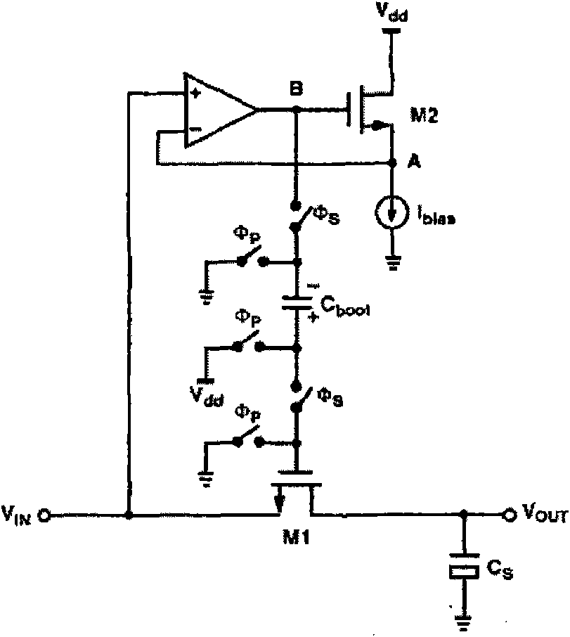
[0081] In order to make the object, technical solution and advantages of the present invention clearer, the present invention will be described in further detail below in conjunction with specific embodiments and with reference to the accompanying drawings.

[0082] The present invention starts from the most basic bootstrap circuit, combines the advantages of existing solutions, and designs a sampling circuit that can work at low voltage, low power consumption, and is insensitive to process errors by using the method of dual bootstrap of gate and substrate voltages. At the same time, the voltage self-compensation method is adopted to eliminate the non-linear problem caused by the clock breakdown after the gate voltage of the switch is bootstrapped.

[0083] Such as Image 6 as shown, Image 6 The structural circuit diagram of the low-voltage high-linearity A / D converter sampling switch based on double bootstrapping and voltage compensation technology provided by the present i...


PUM


Abstract

The invention discloses a dual bootstrap and voltage compensation technology-based A/D converter sampling switch, which comprises a primary switch unit used for a to-be-sampled signal channel to sample to-be-sampled signals, a underlayer voltage bootstrap unit for realizing the underlayer voltage bootstrap of a switching tube PMOS Switch in the primary switch unit, a grid voltage bootstrap unit for realizing the grid voltage bootstrap of the switching tube PMOS Switch in the primary switch unit, a storage unit for parallelly sampling input signals VIN and realizing the temporary storage of a VIN voltage, and a voltage compensation unit for compensating the sampling output voltage of an output end VOUT. The invention provides a sampling switch which is capable of working at low voltage and low power consumption and is insensitive to process errors. Meanwhile, the adopted voltage self-compensation method effectively solves a nonlinear problem caused by clock feedthrough occurring after the grid voltage bootstrap of the switching tube.

Description

technical field [0001] The invention relates to the technical fields of microelectronics and solid electronics, in particular to a low-voltage high-linearity A / D converter sampling switch based on double bootstrap and voltage compensation technologies. Background technique [0002] 1. Bootstrap switch and its accuracy limitations [0003] Analog-to-digital A / D (Analog-to-Digital) converter is an essential interface between analog signal and digital signal in all electronic systems, and its conversion accuracy directly affects the overall performance index of the entire electronic system. [0004] At present, in order to adapt to the rapid development of computer, communication and multimedia technologies, A / D converters have made great progress in technology, structure and performance, and are developing in the direction of low power consumption, high speed and high resolution. The sampling circuit is a crucial unit in the A / D converter, and its performance directly determi...

Claims


Application Information

Patent Timeline
IPC IPC(8): H03M1/06H03M1/12H03K17/14H03K17/687G11C27/02
Inventor 杨海钢刘珂尹韬
Owner INST OF ELECTRONICS CHINESE ACAD OF SCI
Why Eureka
Try Eureka