

Method for actively encapsulating LED chip and encapsulation structure thereof
A technology for LED chips and packaging methods, applied in electrical components, circuits, semiconductor devices, etc., can solve the problems of many processes, air bubbles, and high costs, and achieve the effects of simple packaging equipment, high process repeatability, and short production time.
- Summary
- Abstract
- Description
- Claims
- Application Information
AI Technical Summary
Problems solved by technology
Method used
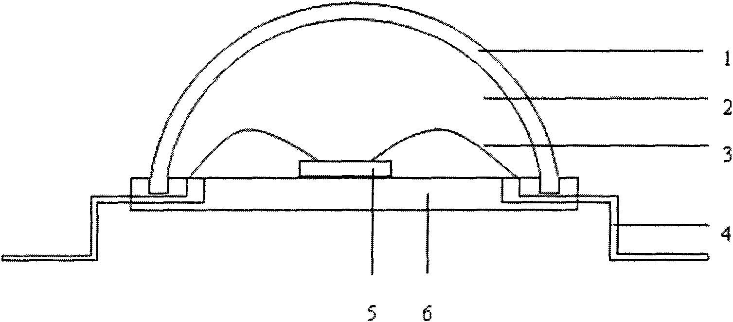
Image

Examples
Embodiment 1
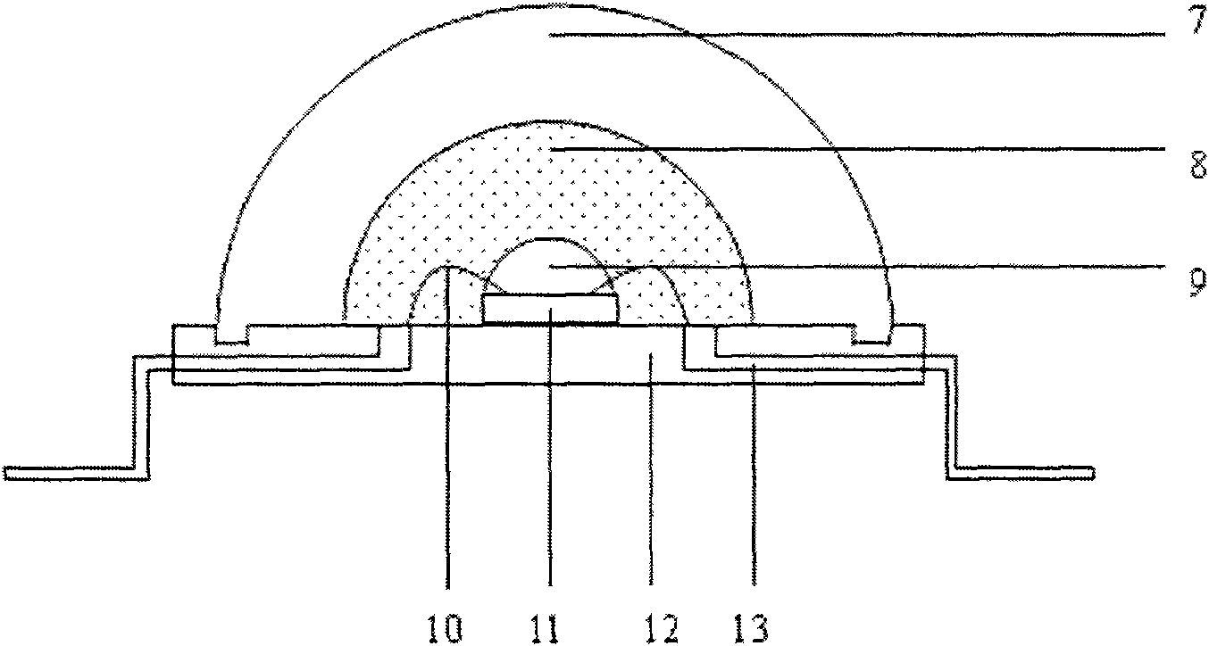
[0042] figure 2 It is a schematic diagram of LED three-layer structure lens embodiment 1 of the present invention, and its structure includes the following parts: LED package support 12 (including support pin 13 and support base), chip 11, gold wire 10 connecting chip and LED support and A lens made of three layers of material. The material of the first layer of lens 9 is the photosensitive resin PE1 configured according to Table 1, the material of the second layer of lens 8 is the photosensitive resin PEP1 mixed with phosphor powder, and the material of the third layer of lens 7 is the same as that of the first layer, also according to Table 1 Configured photosensitive resin PE1.
[0043] The implementation steps of this embodiment are as follows:
[0044] (a) chip 11 is installed in the reflective cup in the LED packaging support 12;
[0045] (b) Complete the circuit connection between the chip and the support by punching gold wires;
[0046] (c) if Figure 4 As shown,...
Embodiment 2
[0063] figure 2 It is also a schematic diagram of Embodiment 2 of the LED three-layer structure lens of the present invention. The difference from Embodiment 1 is that the material of the first layer lens 9 is transparent silica gel (tentatively named S1), and the materials of other layers are the same.
[0064] The implementation steps of this embodiment are as follows:
[0065] (a) chip 11 is installed in the reflective cup in the LED packaging support 12;
[0066] (b) Complete the circuit connection between the chip and the support by punching gold wires;
[0067] (c) if Figure 4 As shown, the LED 22 is placed on the experimental board 21, the electrodes at both ends are connected to the power supply, and the surface of the LED chip 22 is kept parallel to the plane of the experimental board 21, and the LED 22 (that is, the chip 11, the chip base and the packaging support 12) is used. Resin 23 is pre-impregnated to effectively remove the air bubbles on the surface of th...
Embodiment 3
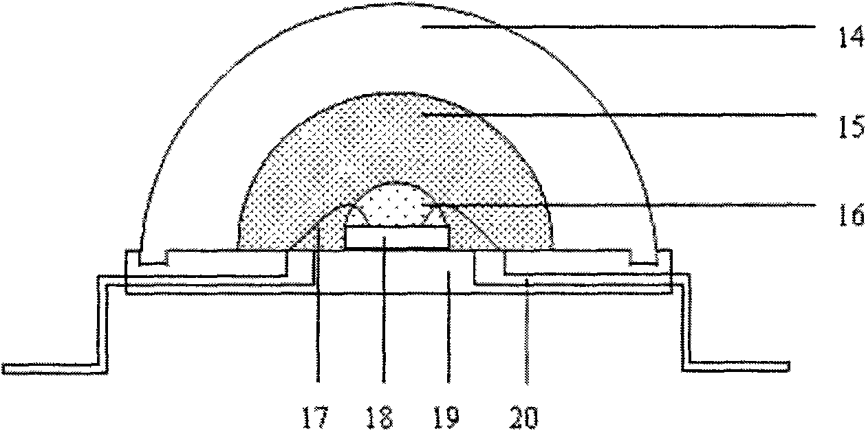
[0082] image 3 It is a schematic diagram of Embodiment 3 of the LED three-layer structure lens of the present invention. The refractive index of the three-layer lens gradually decreases from the inside to the outside, so that the light output efficiency is obviously improved. Its structure includes the following parts: LED packaging bracket 19 (including bracket pins) 20 and support base), chip 18, gold wire 17 connecting the chip and the LED support, and a three-layer structure lens. The material of the first layer of lenses 16 is doped with nanoparticles (such as TiO 2 ) of photosensitive resin (temporarily named PEN1), the material of the second layer of lens 15 is a photosensitive resin mixed with phosphor powder (tentatively named PEP1), and the material of the third layer of lens 14 is undoped photosensitive resin (tentatively named PE1).
[0083] The implementation steps of this embodiment are as follows:
[0084] (a) chip 18 is installed in the reflective cup in the...
PUM
 Abstract
Description
Claims
Application Information