
Eureka
For R&D, Eureka makes reading and utilizing patents & technical documents easy.
Eureka AIR
Designed for self-driven R&D workflows. Generate viable solutions, solve complex R&D challenges, empower your innovation with AI.

Eureka Materials
Designed for material experts only. Revolutionize your material R&D, from search, analyze, to developing new materials.

TechResearch
Generate reliable direction feasibility study reports for your R&D in just a few steps.

TechSeek
Discover and master advanced knowledge NOW. Basics, ideas, possibilities, all at once.

TechMind
As an expert in R&D Theories, TechMind can generates customized viable solutions instantly.

TechRisk
Analyze your overall solution with one click, know your potential R&D risks in advance.

TechMonitor
Get weekly tech updates, stay abreast of the latest tech innovations and key insights.
Material filming device, preparation method and organic electroluminescence component prepared by same
A film-forming device and luminescent technology, applied in the direction of electroluminescent light source, electric light source, electrical components, etc., can solve the problems of affecting production efficiency, unsolvable problems, slow evaporation rate, etc., to increase the bonding force of the film layer, Improve device yield and improve damage effect
- Summary
- Abstract
- Description
- Claims
- Application Information
AI Technical Summary
Problems solved by technology
Method used
Image

Examples
Embodiment 1
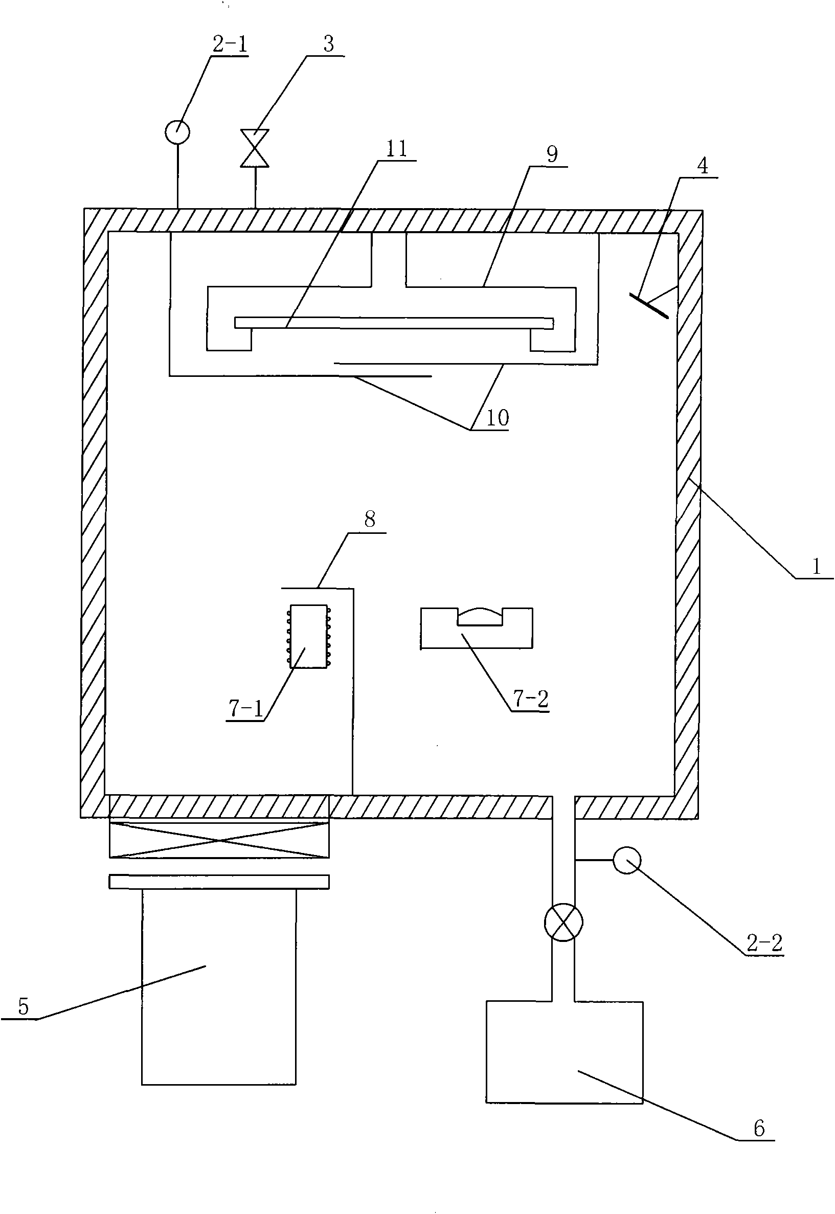
[0046] refer to figure 1 , 2 , 3.
[0047] This embodiment is to prepare organic electroluminescence device, and its device structure is:
[0048] Glass substrate / ITO / NPB(50nm) / Alq 3 (70nm) / Al(300nm)
[0049] (1) Preparation of organic light-emitting layer
[0050] Place the pretreated glass substrate 11 in the vacuum chamber 1, and evacuate to 1×10 -3 Pa, the evaporation hole transport material NPB, the evaporation rate of the material film is 0.1nm / s, and the film thickness is 50nm; on the hole transport layer 22, evaporate 70nm thick Alq 3 As the light-emitting layer and electron transport layer 23 of the device;
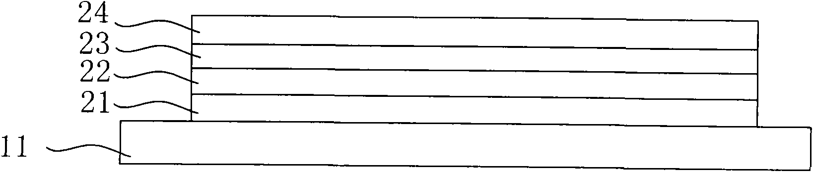
[0051] Wherein the glass substrate 11 is composed of an ITO 21 (indium tin oxide) film and a substrate, the sheet resistance of the ITO film 21 is 50Ω, and the film thickness is 150nm.
[0052] (2) Preparation of cathode layer
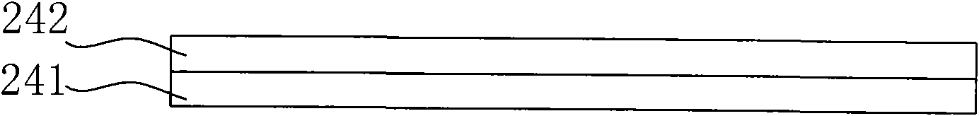
[0053]The evaporation chamber 1 used to prepare this layer is the aforementioned chamber, and the cathode 25 with a film thickne...
Embodiment 2
[0070] refer to figure 1 , 2 , 3.
[0071] This embodiment is to prepare organic electroluminescent devices with different cathode materials, and its device structure is:
[0072] Glass substrate / ITO / NPB(50nm) / Alq 3 (70nm) / Mg(50nm) / Al(250nm)
[0073] (1) Preparation of organic light-emitting layer
[0074] Place the pretreated glass substrate 11 in the vacuum chamber 1, and evacuate to 1×10 -3 Pa, the evaporation hole transport material NPB, the evaporation rate of the material film is 0.1nm / s, and the film thickness is 50nm; on the hole transport layer 22, evaporate 70nm thick Alq 3 As the light-emitting layer and electron transport layer 23 of the device;
[0075] Wherein the glass substrate 11 is composed of an ITO 21 (indium tin oxide) film and a substrate, the sheet resistance of the ITO film 21 is 50Ω, and the film thickness is 150nm.
[0076] (2) Preparation of cathode layer
[0077] The evaporation chamber 1 used to prepare this layer is the aforementioned cham...
Embodiment 3
[0081] refer to figure 2 , 3 , 4.
[0082] This embodiment is to prepare organic electroluminescence device, and its device structure is:
[0083] Glass substrate / ITO / NPB(50nm) / Alq 3 (70nm) / Al(300nm)
[0084] The difference between the preparation device of this embodiment and the evaporation equipment used in Examples 1 and 2 is that a magnetron sputtering source 7-3 is also provided in the evaporation chamber, and two types of the three types of coating sources are used in the cathode of this embodiment— — Resistance heating evaporation source 7-1 and magnetron sputtering source 7-3.
[0085] (1) Preparation of organic light-emitting layer
[0086] Place the pretreated glass substrate 11 in the vacuum chamber 1, and evacuate to 1×10 -3 Pa, the evaporation hole transport material NPB, the evaporation rate of the material film is 0.1nm / s, and the film thickness is 50nm; on the hole transport layer 22, evaporate 70nm thick Alq 3 As the light-emitting layer and electron ...
PUM
| Property | Measurement | Unit |
|---|---|---|
| thickness | aaaaa | aaaaa |
Abstract
Description
Claims
Application Information
 - R&D Engineer
- R&D Manager
- IP Professional
- Industry Leading Data Capabilities
- Powerful AI technology
- Patent DNA Extraction
Browse by: Latest US Patents, China's latest patents, Technical Efficacy Thesaurus, Application Domain, Technology Topic, Popular Technical Reports.
© 2024 PatSnap. All rights reserved.Legal|Privacy policy|Modern Slavery Act Transparency Statement|Sitemap|About US| Contact US: help@patsnap.com