
Method for preparing high-voltage SIDAC

A bidirectional trigger and diode technology, which is applied in semiconductor/solid-state device manufacturing, electrical components, circuits, etc., can solve the problems of low reliability of diodes, high requirements for manufacturing conditions, and high production costs, so as to enhance anti-ablation ability and reduce Production cost, the effect of improving product quality

Active Publication Date: 2011-02-16
常州银河电器有限公司
View PDF0 Cites 1 Cited by
  • Summary
  • Abstract
  • Description
  • Claims
  • Application Information

AI Technical Summary

Problems solved by technology

The existing production methods have the following disadvantages: ① due to the need for multiple times of glass firing and photolithography, the production steps are numerous and complicated; ② due to the use of chemical and mechanical polishing, not only the production cost is high, but also the silicon can be damaged. ③Because photolithography must be manufactured in an environment of 1000 or higher, so the production conditions are relatively high, which also leads to high costs; The corrosion ability is lower, making the reliability of the diode lower

Method used

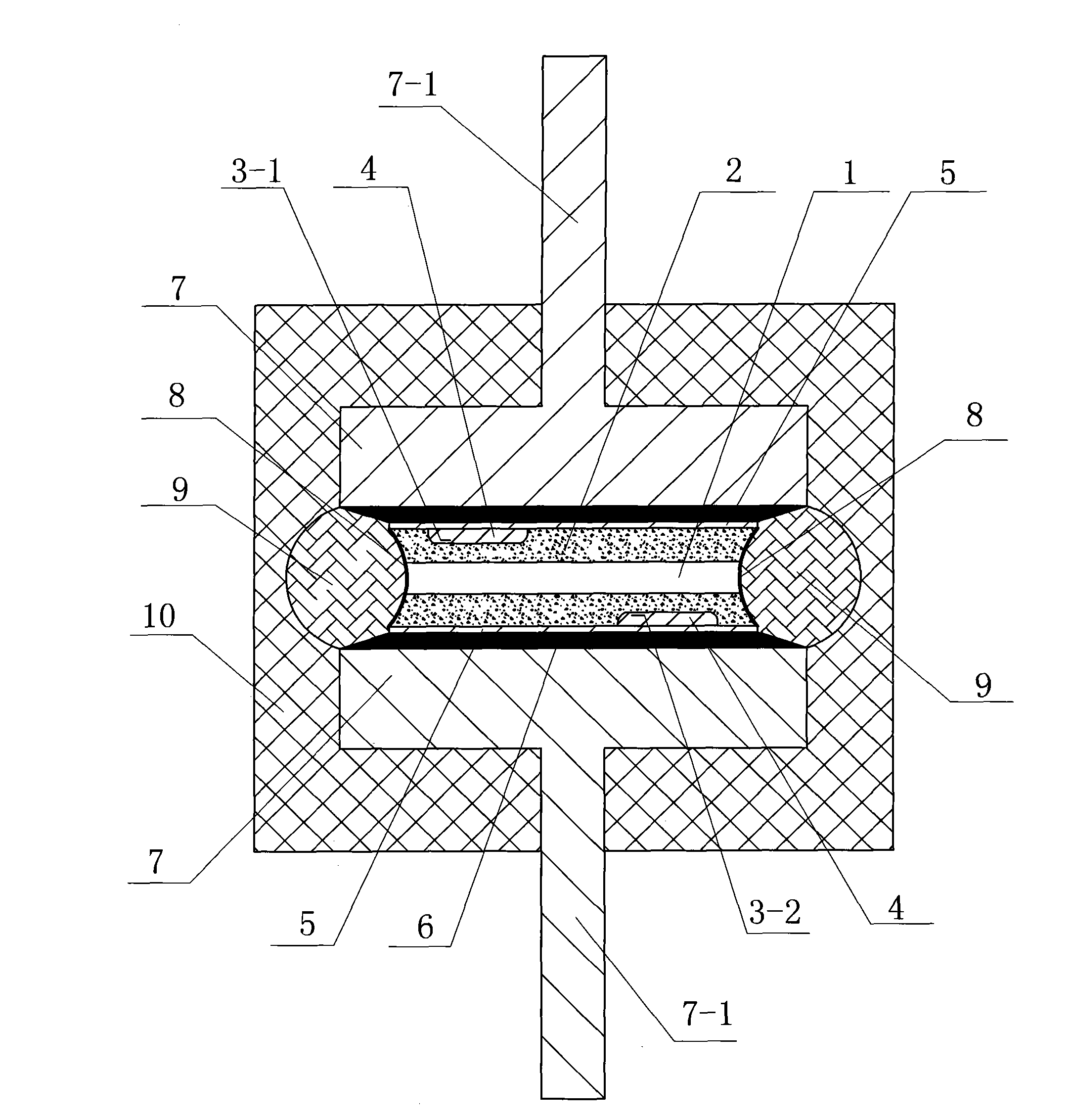
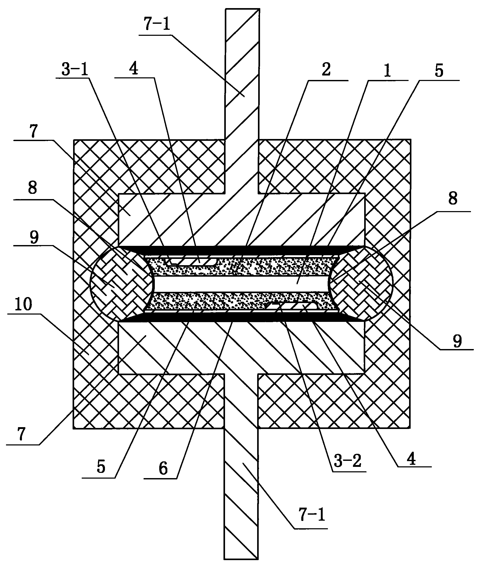

Image

  • Method for preparing high-voltage SIDAC
  • Method for preparing high-voltage SIDAC

Examples


Embodiment

[0044] Example: Making a high-voltage bidirectional trigger diode

[0045] (1) Prepare raw materials:

[0046] ①Preparation of silicon wafers: Cut the purchased N-type single crystal rods into circular shapes as raw silicon wafers, with a resistivity of ρ=4±1Ω.cm and a thickness of 200±10μm;

[0047] ② Prepare the etching solution used in the chemical polishing step: mix evenly according to the volume ratio of hydrofluoric acid, glacial acetic acid and nitric acid 1:1:2:27;

[0048]3. prepare the rinsing solution used in the nickel plating and alloying steps: mix evenly in the proportion of hydrofluoric acid: deionized water=1:15;

[0049] ④ Prepare the nickel plating solution A used in the nickel plating and alloying steps: nickel chloride: ammonium chloride: diammonium hydrogen citrate: sodium hypophosphite: deionized water = 30g: 50g: 65g: 10g: 1000ml than mixing evenly;

[0050] ⑤ Prepare the mixed acid solution used in the pickling step: mix evenly according to the vol...


PUM

PropertyMeasurementUnit
thicknessaaaaaaaaaa
thicknessaaaaaaaaaa
thicknessaaaaaaaaaa

Abstract

The invention relates to a method for preparing a high-voltage diac. In the method, a raw material silicon chip is processed in sequence by the following steps: chemical polishing, boron diffusion, oxidation of a mask, double-sided primary photoetching, phosphorous diffusion, nickel plating and alloying, scribing, welding, acid washing, protection, and packaging to obtain a finished product of the high-voltage diac, wherein the chemical polishing step is that the raw material silicon chip is evenly corroded in corrosion solution at the normal temperature for 3 to 5 minutes, washed for multiple times and dried to obtain a silicon chip (1) with the matt surface, and the corrosion solution is formed by mixing hydrofluoric acid, glacial acetic acid and nitric acid according to the volume ratio of 1:1 to 3:25 to 30; and the acid washing step is that a corrosion layer (8) is formed on the periphery of the silicon chip (1) obtained by soaking by mixed acid liquor, corroding and welding so asto obtain the electric performance, and the mixed acid solution is formed by mixing the hydrofluoric acid, the nitric acid, acetic acid and sulfuric acid according to the volume ratio of 9: 9: 9 to 15:4. The method has the advantages of simplified working procedure, low cost, reliable performance and corrosion resistance.

Description

technical field [0001] The invention relates to a method for manufacturing a high-voltage bidirectional trigger diode, and the prepared diode is especially suitable for starting high-voltage neon lamps and lighting circuits. Background technique [0002] At present, the electrical industry is developing in the direction of high integration, high voltage, and high power. Existing methods for making high-voltage bidirectional trigger diodes include chemical and mechanical polishing, boron diffusion, oxidation, primary photolithography, phosphorous diffusion, secondary photolithography, primary glass firing, secondary glass firing, triple photolithography, and metal evaporation , dicing, pickling and encapsulation to produce products. The existing production methods have the following disadvantages: ① due to the need for multiple times of glass firing and photolithography, the production steps are numerous and complicated; ② due to the use of chemical and mechanical polishing,...

Claims


Application Information

Patent Timeline
Patent Type & Authority Patents(China)
IPC IPC(8): H01L21/329H01L21/306
Inventor 王兴龙唐国琴孙良
Owner 常州银河电器有限公司
Learn More