Image display system and manufacture method thereof

A technology of an image display system and a manufacturing method, which is applied in the manufacture of semiconductor/solid-state devices, radiation control devices, electrical components, etc., can solve the problems of inability to improve yield, long process time, uneven light emission, etc.

Inactive Publication Date: 2009-12-02
INNOLUX CORP
View PDF0 Cites 12 Cited by
  • Summary
  • Abstract
  • Description
  • Claims
  • Application Information

AI Technical Summary

Problems solved by technology

[0005] However, compared to the crystallization process performed by a single laser crystallization technology, the above-mentioned various methods of different crystallization processes not only have a longer process time, but also have a complicated process, so there is still the difficulty that the yield cannot be improved.
In addition, polysilicon produced by different crystallization processes will also cause obvious differences in grain characteristics. The present invention aims to solve the phenomenon of uneven light emission (Mura) caused by the differences between OLEDs, which causes the yield rate of AMOLED products to vary. low problem

Method used


Image

  • Image display system and manufacture method thereof
  • Image display system and manufacture method thereof
  • Image display system and manufacture method thereof

Examples


Embodiment Construction

[0017] The technical content of the present invention will be described in detail below with reference to the accompanying drawings.

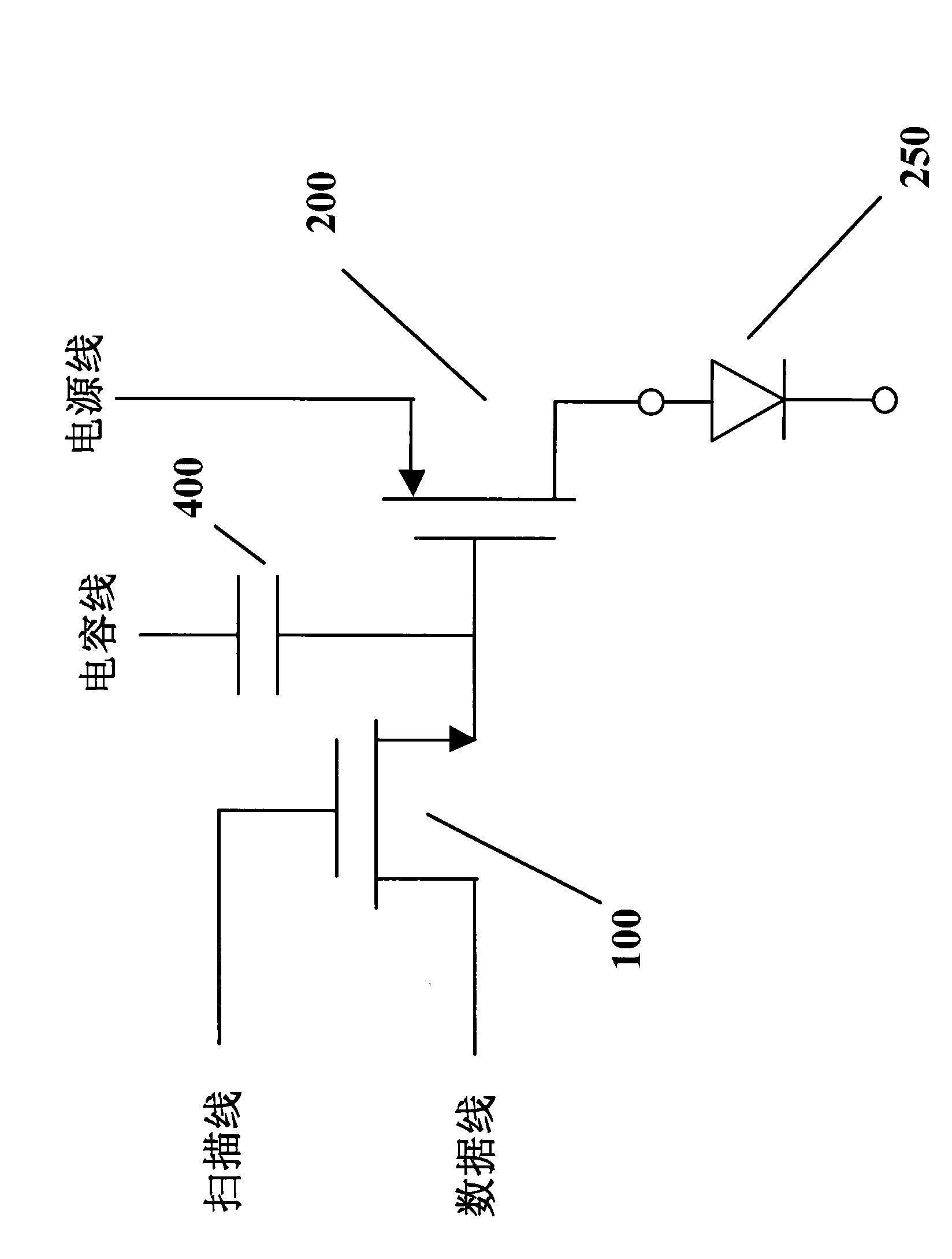
[0018] Please refer to figure 1 , which shows a simple structure diagram of an active matrix organic light emitting diode display (AMOLED). A pixel unit of an active matrix organic light emitting diode (AMOLED) display may include a switching TFT 100 , a driving TFT 200 , a light sensing element 250 and a capacitor 400 .

[0019] As mentioned above, the requirements for its electrical performance are quite different: for switching TFTs, low sub-threshold swing and high carrier mobility are required. For driving TFTs, a high sub-threshold swing is required to meet the requirement of uniformity among transistors, so as to transmit the conduction current for driving the photo-sensing element 250 . However, the current driving is very sensitive to the difference of the individual photo-sensing elements 250 , and the existence of the difference be...


PUM


Abstract

The invention relates to an image display system and a manufacture method thereof. The image display system comprises a basal plate, a switch film transistor, a driving film transistor, a light-sensing component and a capacitor, wherein a baffle layer is formed on the basal plate; no conductive layer is formed in a first section predicted to form the switch film transistor so as to form a shielding layer; and a conductive layer is formed in a second section predicted to form the driving film transistor, the light-sensing component and the capacitor so as to form the shielding layer. Weather the conductive layer exists or not in the single crystallized processing procedure and the thermal conductive phenomenon of a quasimolecule laser annealing method are utilized to form polycrystalline silicon layers with different grain sizes in the first section and the second section so that the image display system has favorable uniformity of luminance.

Description

technical field [0001] The present invention relates to an image display system and a manufacturing method thereof, in particular to an Active Matrix Organic Light Emitting Diode (AMOLED) display circuit and a manufacturing method thereof. Background technique [0002] Organic Light Emitting Diode (OLED) has been recognized as the flat panel display technology of the next era, especially Active Matrix Organic Light Emitting Diode (AMOLED) display, which is a product that relevant industries are investing a lot of resources in developing. A pixel unit of an active matrix organic light emitting diode (AMOLED) display may include a driving TFT, a switching TFT, a light sensing element and a capacitor. When making the aforementioned AMOLED components, the Amorphous Silicon layer (Amorphous Silicon) grown on the glass substrate is transformed into a polysilicon layer (Poly Silicon) by using Excimer Laser Anneal (ELA). [0003] However, due to the different electrical performance...

Claims


Application Information

Patent Timeline
Patent Type & Authority Applications(China)
IPC IPC(8): H01L21/84H01L27/12H01L27/144H01L27/32
Inventor 刘侑宗李淂裕
Owner INNOLUX CORP
Why Eureka
Try Eureka