Memory cell of resistive random access memory (RRAM) and preparation method thereof
A technology of random access memory and storage unit, applied in electrical components, ion implantation plating, coating and other directions, can solve the problem of less research on resistive random access memory, and achieve the effect of excellent transformation and memory characteristics and good stability
- Summary
- Abstract
- Description
- Claims
- Application Information
AI Technical Summary
Problems solved by technology
Method used
Image
Examples
Embodiment Construction
[0025] The present invention will be further described in detail below in conjunction with the accompanying drawings and embodiments.
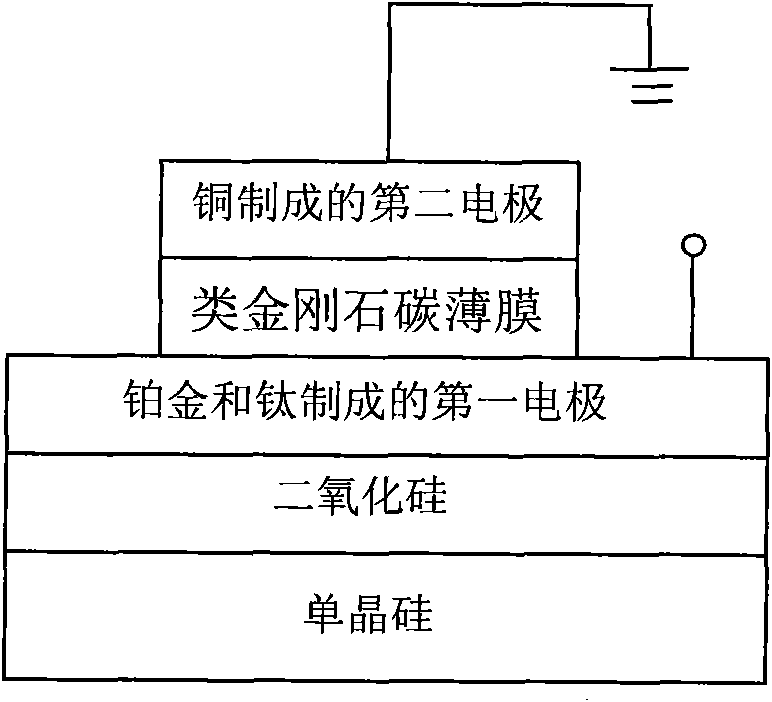
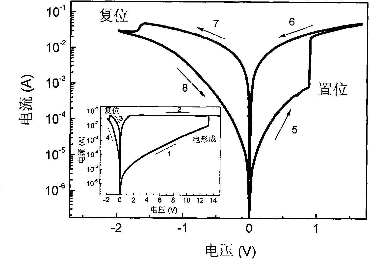
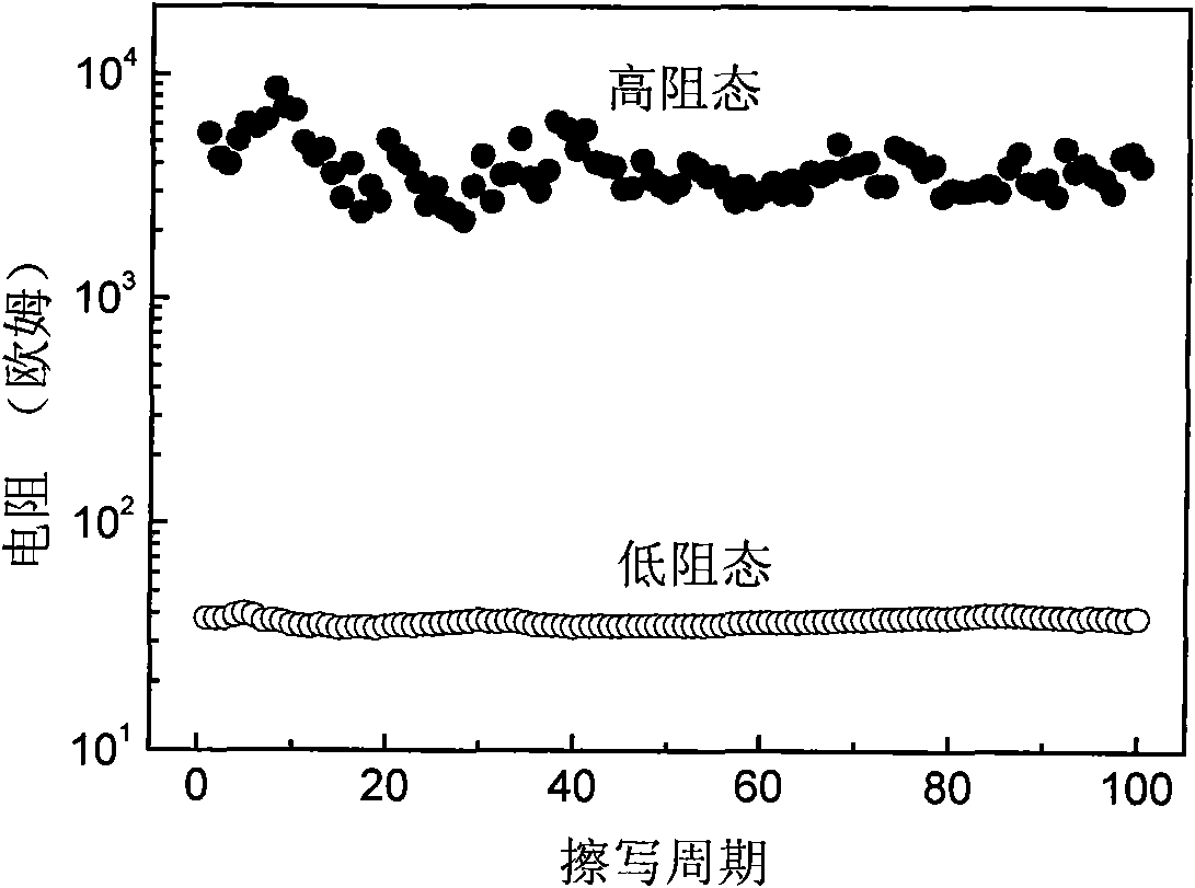
[0026] Such as figure 1 The storage unit of the resistive random access memory shown includes an insulating substrate, the insulating substrate is composed of single crystal silicon and a silicon dioxide isolation dielectric layer grown on the surface of the single crystal silicon, and the first electrode is arranged on the silicon dioxide isolation dielectric layer , the first electrode is made up of platinum with a thickness of 200nm and titanium with a thickness of 50nm; an intermediate layer of a diamond-like carbon film doped with chromium is set on the surface of the first electrode, and the atomic percentage of chromium in the diamond-like carbon film is 1.3%. The thickness of the layer is 130 nm, and a second electrode made of copper is arranged on the surface of the intermediate layer, and the thickness of the second electrode is 200 ...
PUM
 Abstract
Description
Claims
Application Information
 - R&D
- Intellectual Property
- Life Sciences
- Materials
- Tech Scout
- Unparalleled Data Quality
- Higher Quality Content
- 60% Fewer Hallucinations
Browse by: Latest US Patents, China's latest patents, Technical Efficacy Thesaurus, Application Domain, Technology Topic, Popular Technical Reports.
© 2025 PatSnap. All rights reserved.Legal|Privacy policy|Modern Slavery Act Transparency Statement|Sitemap|About US| Contact US: help@patsnap.com


