Sapphire substrate and polishing method and application thereof

A sapphire substrate, sapphire technology, applied in electrical components, electrical solid devices, circuits, etc., can solve the problems of reducing the quantum luminous efficiency of the device, affecting the performance of the device, and high cost, increasing the internal quantum luminous efficiency and reducing the dislocation density. , the effect of alleviating stress concentration

Active Publication Date: 2009-12-16
SHANGHAI XINANNA ELECTRONICS TECH
View PDF0 Cites 9 Cited by
  • Summary
  • Abstract
  • Description
  • Claims
  • Application Information

AI Technical Summary

Problems solved by technology

Such surface processing usually requires multiple grinding and polishing processes (coarse grinding, fine grinding, rough polishing, fine polishing), especially surface precision polishing, which is difficult, costly and time-consuming
At the same time, there is a large lattice mismatch (≈16%) between sapphire and GaN materials. Even the epitaxial layer grown on the most perfect substrate surface has a large number of dislocations and even cracks. These defects will greatly reduce the internal stability of the device. Quantum luminous efficiency (internal quantum efficiency), affecting device performance
[0004] On the other hand, because the refractive index of GaN-based materials is greater than that of aluminum oxide, the photons excited by the working layer of the device are not easy to be exported from the inside of the device due to total reflection, which directly leads to the difficulty in improving the light extraction efficiency of the diode; a large number of photons generated After multiple total reflections inside the device, it is released in the form of heat, which is not conducive to the long-term stable operation of the light-emitting device

Method used


Image

  • Sapphire substrate and polishing method and application thereof
  • Sapphire substrate and polishing method and application thereof
  • Sapphire substrate and polishing method and application thereof

Examples


Embodiment 1

[0030] 1) cutting to obtain a sapphire single crystal substrate sheet with a thickness of 300 microns;

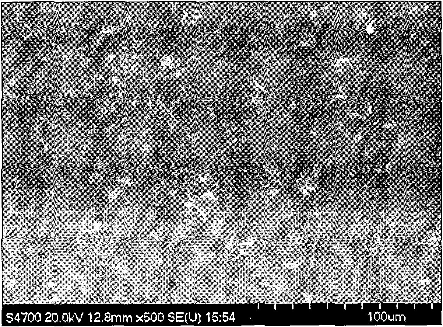
[0031] 2) Grinding with boron carbide with a particle size of about 1 micron until the thickness difference in the chip is reduced to less than 1 micron, and ultrasonically cleaning to obtain a sapphire substrate grinding chip with a rough structure on the surface, such as figure 1 shown;

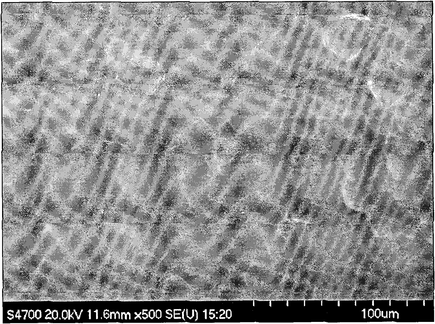
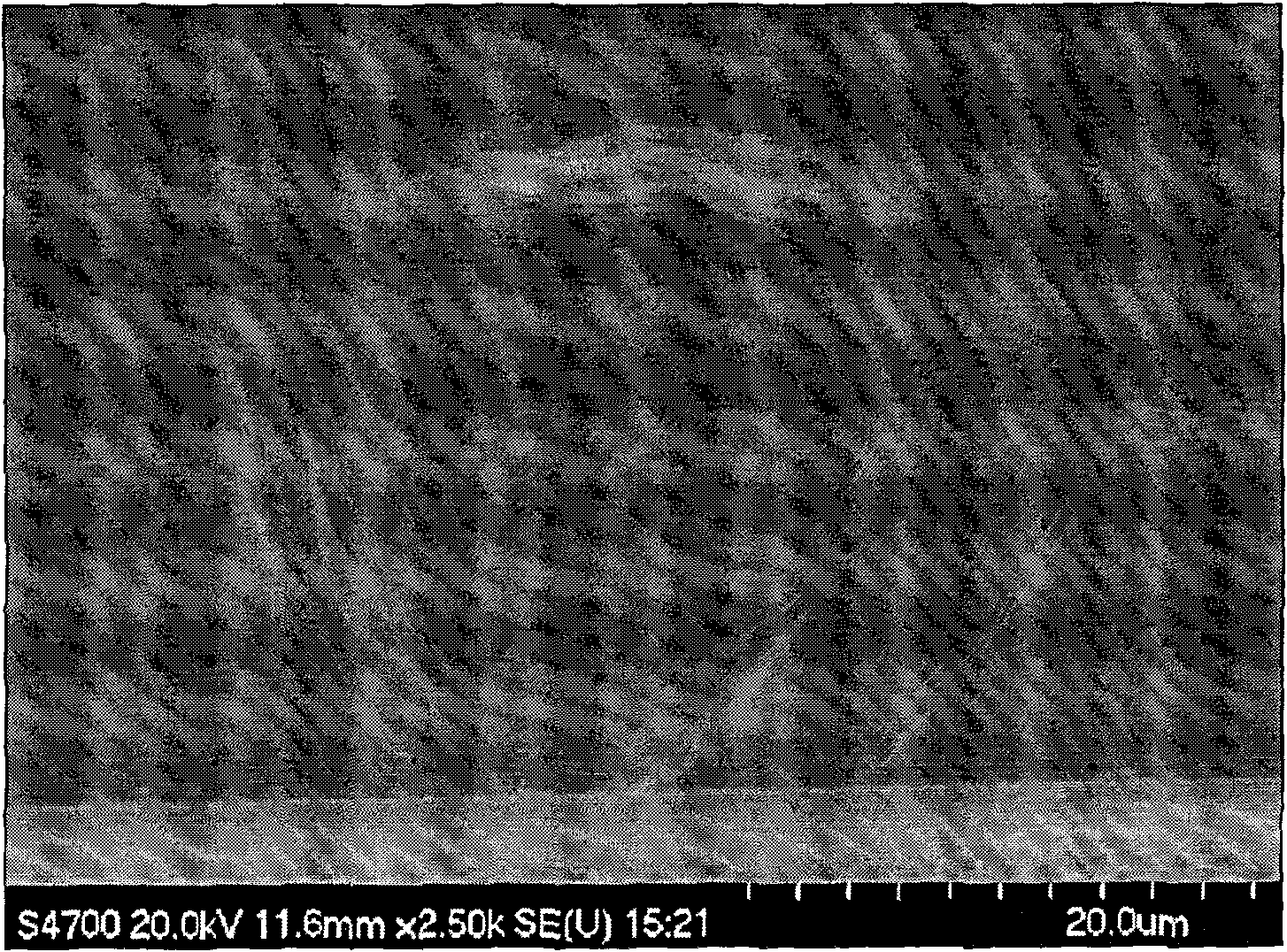
[0032] 3) Etching the sapphire substrate grinding piece in the polishing agent to perform chemical polishing directly, the polishing temperature is 150 degrees Celsius, the polishing time is 24 hours, and the polishing pressure is about 0.5 MPa. The polishing agent is a mixture of NaOH and KOH, and their weight ratio is 1:1. The obtained substrate surface is as figure 2 and image 3 shown. The polished surface has a random and disordered concave pattern structure, the lateral dimension of the pattern depression is 10-30 microns, the vertical depth is 500 nanometers-2 microns, and th...

Embodiment 2

[0034] 1) cutting to obtain a sapphire single crystal substrate sheet with a thickness of 500 microns;

[0035] 2) Grinding with diamond with a particle size of about 0.5 micron until the thickness difference in the chip is reduced to less than 1 micron, and ultrasonically cleaning to obtain a sapphire substrate grinding chip with a rough structure on the surface;

[0036] 3) Etching the sapphire substrate grinding piece in the polishing agent to perform chemical polishing directly, the polishing temperature is 200 degrees Celsius, the polishing time is 18 hours, and the polishing pressure is about 1.0 MPa. The polishing agent contains NaOH, KOH, Na 2 SO 4 mixture, the weight fraction between them is 3:3:1. The obtained substrate surface has a random and disordered concave pattern structure, such as Figure 4 and Figure 5 shown. The lateral size of the depression in the pattern is 2-10 micrometers, the vertical depth is 100-500 nanometers, and the percentage of the surfa...

Embodiment 3

[0038] 1) cutting to obtain a sapphire single crystal substrate sheet with a thickness of 800 microns;

[0039] 2) Grinding with boron carbide with a particle size of about 3 microns until the thickness difference in the chip is reduced to less than 1 micron, and ultrasonically cleaning to obtain a sapphire substrate grinding chip with a rough structure on the surface;

[0040] 3) Etching the sapphire substrate grinding piece in the polishing agent to perform chemical polishing directly, the polishing temperature is 400 degrees Celsius, the polishing time is 4 hours, and the polishing pressure is about 10 MPa. The polishing agent is a mixture of NaOH, KOH and LiOH, and the weight ratio among them is 2:2:1. The surface of the obtained substrate has a random and disordered concave pattern structure, the lateral dimension of the pattern depression is 1-5 micrometers, the vertical depth is 50-100 nanometers, and the percentage of the surface area of ​​the sapphire substrate is 50%...


PUM

PropertyMeasurementUnit
sizeaaaaaaaaaa
depthaaaaaaaaaa
depthaaaaaaaaaa

Abstract

The invention relates to the field of semiconductor materials and discloses a sapphire substrate and a polishing method and an application thereof. The surface of the sapphire substrate is polished, and the polished surface has random sunken patterns. The surface of the sapphire substrate is partially planarized. Therefore the processing cost for the sapphire substrate is greatly reduced and the polishing efficiency is increased.

Description

technical field [0001] The invention relates to the field of semiconductor materials, in particular to a semiconductor substrate material, a sapphire substrate, and a polishing method and application thereof. Background technique [0002] Sapphire is α-Al 2 o 3 The single crystal belongs to the hexagonal crystal system, and the lattice constant is: Widely used in the epitaxial growth of thin film materials and window materials. Sapphire has stable chemical properties, high hardness, and difficult surface processing. As a substrate material for group III-V compound semiconductors (such as GaN), sapphire is widely used in the manufacturing process of light emitting diode (light emitting diode, LED) and laser diode (laser diode, LD) devices. [0003] Traditionally, in order to prepare high-quality epitaxial films and improve the luminous efficiency of devices, the surface of sapphire substrate wafers must be polished to achieve nanoscale global planarization. Such surfa...

Claims


Application Information

Patent Timeline
Patent Type & Authority Applications(China)
IPC IPC(8): H01L23/00H01L21/304H01L21/306
Inventor 胡晓凯宋志棠刘卫丽
Owner SHANGHAI XINANNA ELECTRONICS TECH
Why Eureka
Try Eureka