Exposure mask using gray-tone pattern, manufacturing method of tft substrate using the same and liquid crystal display device having the tft substrate
A technology of gray tone mask and manufacturing method, which is applied in the direction of photolithography exposure device, microlithography exposure equipment, originals for photomechanical processing, etc., and can solve the problem of different methods and effects, distorted resist pattern shape, The narrowing of the width and other issues can achieve the effects of reducing display defects, improving the half-thickness uniformity of the resist, and improving the manufacturing yield
- Summary
- Abstract
- Description
- Claims
- Application Information
AI Technical Summary
Problems solved by technology
Method used
Image
Examples
Embodiment approach 1
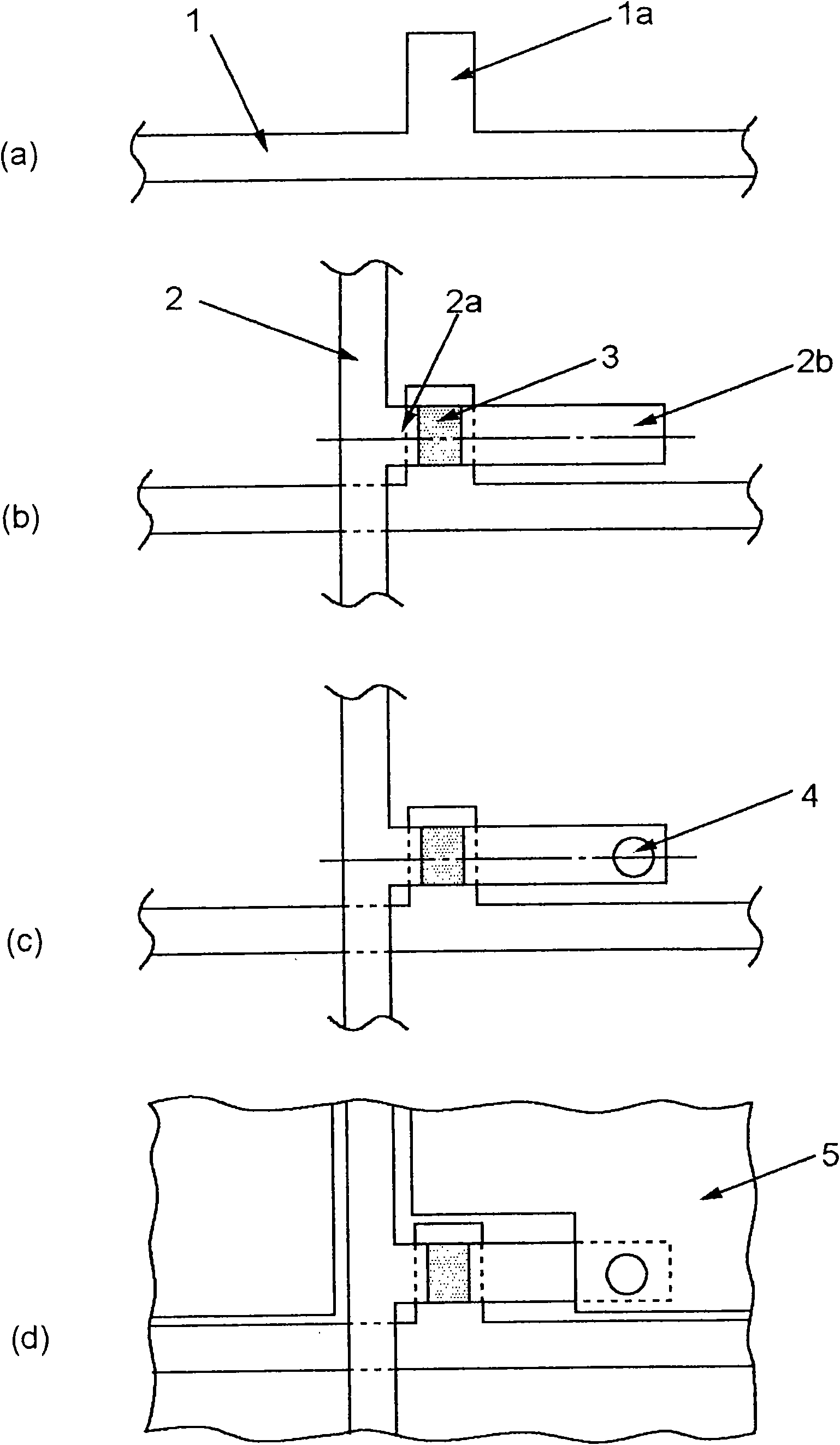
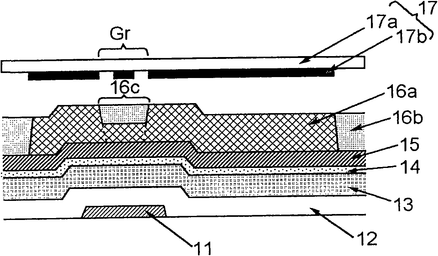
[0090] First, on a transparent glass substrate, metal such as Cr, Mo, Al, and their alloys are formed into a film by sputtering, and the gate wiring 1, the gate electrode 1a, and the gate terminal are formed in the first photolithography step. sub (not shown) ( figure 1 (a)). Next, if Figure 3A As shown in the cross-sectional view of the gate electrode 11, the SiNx film 12 constituting the gate insulating film, the a-Si layer 13 constituting the semiconductor layer, and the n-Si layer constituting the ohmic contact layer are stacked on the gate electrode 11 by the CVD method and the sputtering method respectively. + a-Si layer 14, metal layer 15 such as Cr, Mo, Al and their alloys. Next, in a second photolithography step using a gray tone mask, a source electrode, a drain electrode, a drain wiring, a drain terminal (not shown), and an island are sequentially formed.
[0091] This second photolithography step will be described in further detail. In the second photolithogra...
Embodiment approach 2
[0099] The liquid crystal display device is constituted by sandwiching a liquid crystal layer between an active matrix substrate 101 on which a plurality of pixel electrodes are formed and a counter substrate 102 on which counter electrodes are formed. Such as Figure 11 As shown, on the active matrix substrate 101, a plurality of scanning lines 103 (G1 to G9, ...) and a plurality of data lines 104 (D1 to D9, ...) are arranged to cross each other. A plurality of pixel electrodes 105 are arranged in an area surrounded by the line 103 and the plurality of data lines 104 . The scanning line 103 and the data line 104 are connected to the pixel electrode 105 through the pixel Tr as shown in Embodiment Mode 1.
[0100] Further, on the peripheral region P of the active matrix substrate 101, wiring patterns for driving ICs mounted in the COG format or the COF format are arranged. This wiring pattern is a control signal wiring and / or a power supply wiring for the driving IC. The wir...
PUM
 Abstract
Description
Claims
Application Information


