Preparation method of hollow medical metal micro-needle

A micro-needle and metal technology, applied in the directions of micro-needles, needles, and drug devices, can solve the problems of easy breakage, high cost, and the needle tip is not sharp, and achieve the effect of good mechanical properties, low processing cost, and improved effect.

Inactive Publication Date: 2010-01-13
SHANGHAI JIAO TONG UNIV
View PDF0 Cites 21 Cited by
  • Summary
  • Abstract
  • Description
  • Claims
  • Application Information

AI Technical Summary

Problems solved by technology

However, this method uses microneedles processed by deep reactive ion etching, which is costly; the microneedles are made of silicon material and

Method used


Image

  • Preparation method of hollow medical metal micro-needle
  • Preparation method of hollow medical metal micro-needle
  • Preparation method of hollow medical metal micro-needle

Examples


Embodiment 1

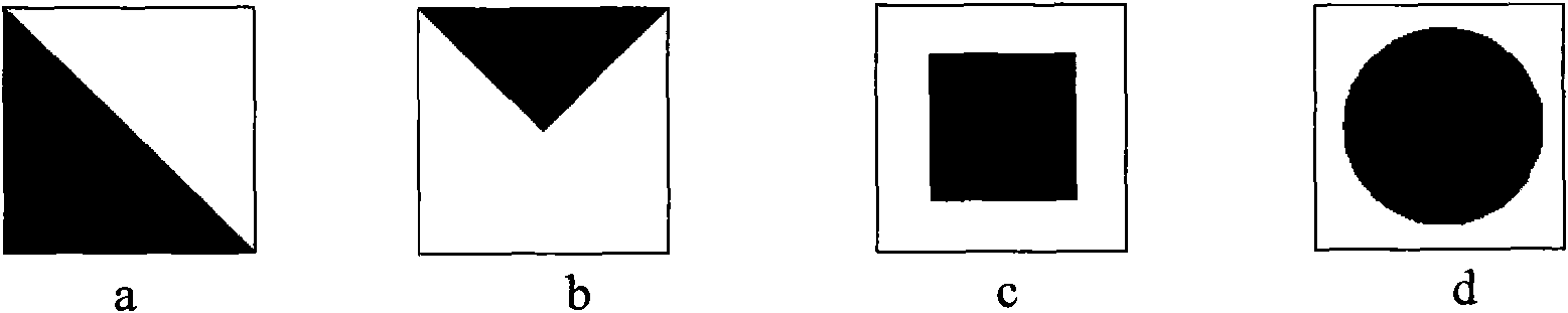
[0033] Such as figure 1 a and figure 2 As shown, in this embodiment, a right-angled triangular mask is used to form oblique triangular truss microneedles when removing the negative glue that fills the silicon pit.

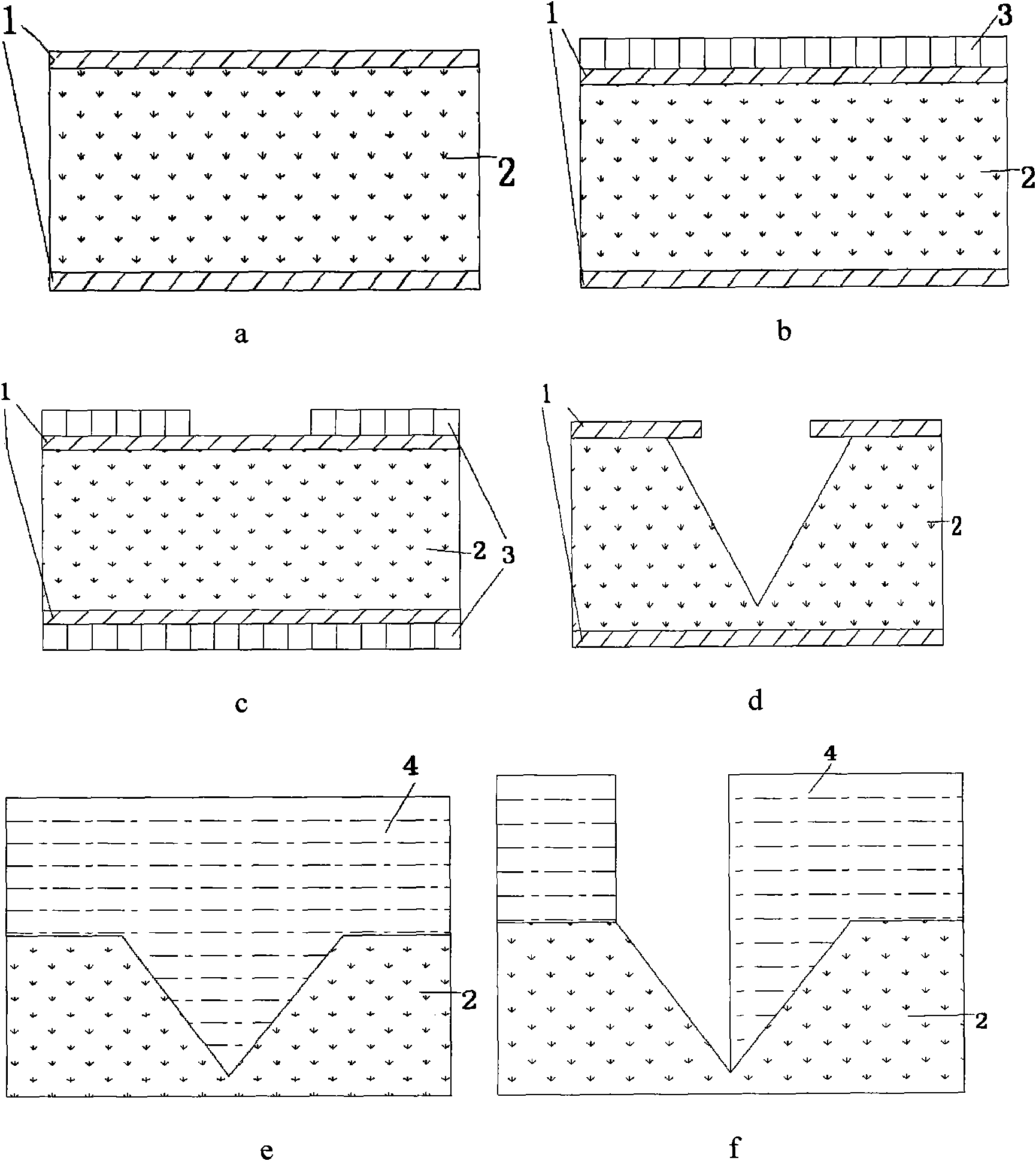
[0034] 1. Bake the double-polished silicon oxide wafer in an oven at 180°C for 3 hours, then spin-coat a photoresist positive resist of 5 μm on the front side of the double-polished silicon oxide wafer, and then bake at 95°C for 30 minutes. figure 1 As shown in a, wherein: the silicon dioxide layer 1 is located on both sides of the silicon 2, and its thickness is 2-3 μm;

[0035] 2. Use the mask plate with the target pattern to expose, and open a square photoresist positive window with a side length of 350 μm after development, such as figure 1 As shown in b, 3 is the photoresist positive resist layer;

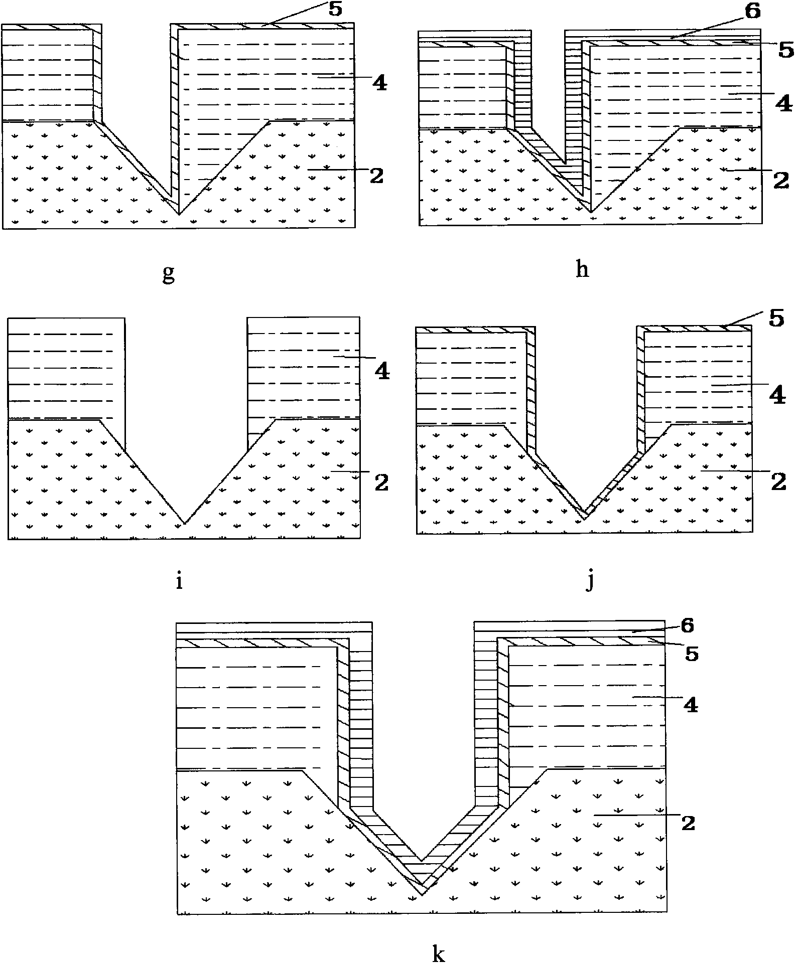
[0036] 3. Bake at 90°C for 30 minutes, and then throw a layer of photoresist positive resist on the back of the double-polished silicon oxide wafer, with a thi...

Embodiment 2

[0053] Such as figure 1 b and figure 2 As shown, in this embodiment, an oblique triangular mask is used to form a right-angled triangular truss microneedle when removing the negative resist that fills the silicon pit.

[0054] 1. Bake the double-polished silicon oxide wafer in an oven at 180°C for 3 hours, then spin-coat a photoresist positive resist of 5 μm on the front side of the double-polished silicon oxide wafer, and then bake at 95°C for 30 minutes. figure 2 As shown in a, wherein: silicon dioxide layer 1 is located on both sides of silicon 2, and its thickness is 2.5 μm;

[0055] 2. Use the mask plate with the target pattern to expose, and open a square photoresist positive window with a side length of 350 μm after development, such as figure 2 As shown in b, 3 is the photoresist positive resist layer;

[0056] 3. Bake at 90°C for 30 minutes, and then throw a layer of photoresist positive resist on the back of the double-polished silicon oxide wafer, with a thick...

Embodiment 3

[0073] Such as figure 1 c and figure 2 As shown, in this embodiment, a square mask is used to form a square-shaped microneedle when removing the negative glue that fills the silicon pit. The specific steps are as follows:

[0074] 1. Bake the double-polished silicon oxide wafer in an oven at 180°C for 3 hours, then spin-coat a photoresist positive resist of 5 μm on the front side of the double-polished silicon oxide wafer, and then bake at 95°C for 30 minutes. figure 1 As shown in a, wherein: the silicon dioxide layer 1 is located on both sides of the silicon 2, and its thickness is 2-3 μm;

[0075] 2. Expose with a mask plate with the target pattern ready, and open a square photoresist window with a side length of 350 μm after development, such as figure 1 As shown in b, 3 is the photoresist positive resist layer;

[0076] 3. Bake at 90°C for 30 minutes, and then throw a layer of photoresist positive resist on the back of the double-polished silicon oxide wafer, with a th...


PUM

PropertyMeasurementUnit
Depthaaaaaaaaaa
Thicknessaaaaaaaaaa
Depthaaaaaaaaaa

Abstract

The invention relates to a preparation method of a hollow medical metal micro-needle, which belongs to the technical field of biomedical engineering. The preparation method comprises the steps of firstly opening a silicon etching window on a double-throw oxide silicon wafer by lithography, wet-etching silicon in the window for obtaining a pyramid-shaped cavity, then throwing a negative photoresist on the silicon wafer for filling the pyramid-shaped cavity, adjusting the height of the micro-needle through the thickness of the negative photoresist, then selecting a specific mask for exposing and removing the negative photoresist in the pyramid-shaped cavity, obtaining a micro-needle cavity with different shape, sputtering a metal thin film in the micro-needle cavity as a conducting layer, electroplating a metal layer on the conducting layer, finally opening a micro-needle through hole in the micro-needle, removing the silicon and the negative photoresist, and further obtaining the hollow metal micro-needle with the different shape. The preparation method adopts the silicon and non-silicon compounding method for preparing the hollow metal micro-needle, and the processing cost is low. The shape of a needle tip of the micro-needle can be controlled by exposure, thereby improving the effect of inserting the micro-needle into skin, effectively controlling the height of the micro-needle and improving the strength of the micro-needle.

Description

technical field [0001] The invention relates to a method for preparing microneedles in the technical field of biomedical engineering, in particular to a method for preparing hollow medical metal microneedles. Background technique [0002] The use of microneedles for transdermal drug delivery is a new way to introduce drugs into living organisms. Usually microfabrication technology is used to make solid or hollow microneedle arrays of hundreds of microns. The micro-needle is thin and sharp, and the general puncture depth is only in the stratum corneum and epidermis, without touching the nerve endings. The micro-tip also greatly reduces the probability of the needle tip touching the nerve endings, and reduces the degree of damage to the corresponding accessory tissues of the body. , does not produce pain, so it is a painless administration method. The microneedle is small in size, so it causes less trauma to the organism, and the formed wound recovers quickly; the operation ...

Claims


Application Information

Patent Timeline
IPC IPC(8): A61M37/00
CPCA61M37/0015A61M2037/003A61M2037/0053
Inventor 刘景全闫肖肖杨春生唐刚芮岳峰
Owner SHANGHAI JIAO TONG UNIV
Why Eureka
Try Eureka