Eureka AIR delivers breakthrough ideas for toughest innovation challenges, trusted by R&D personnel around the world.

Silicon dielectric treating agent for use after etching, process for producing semiconductor device, and semiconductor device

A technology of post-treatment agent and manufacturing method, which is applied in semiconductor/solid-state device manufacturing, semiconductor device, preparation of detergent mixture composition, etc., can solve problems such as increased dielectric constant and poor adhesion, and achieves improved Effects of manufacturing yield, suppression of increase in dielectric constant, and quality improvement

Inactive Publication Date: 2013-10-30
FUJITSU LTD
View PDF1 Cites 0 Cited by
  • Summary
  • Abstract
  • Description
  • Claims
  • Application Information

AI Technical Summary

Problems solved by technology

However, the surface of silicon compound-based materials is hydrophilized by etching during the formation of multilayer wiring, and the dielectric constant increases (etching damage) due to the influence of water absorption, and the dielectric constant increases due to etching residues. and poor adhesion to the upper layer

Method used


Image

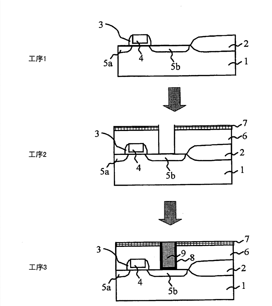
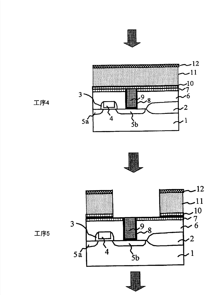
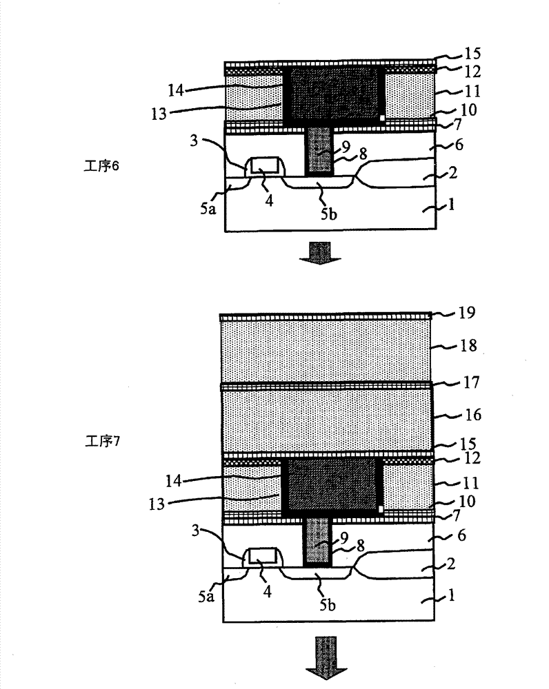
  • Silicon dielectric treating agent for use after etching, process for producing semiconductor device, and semiconductor device
  • Silicon dielectric treating agent for use after etching, process for producing semiconductor device, and semiconductor device
  • Silicon dielectric treating agent for use after etching, process for producing semiconductor device, and semiconductor device

Examples


Embodiment 1

[0120] Add 118g (1.0mol) of trimethylethoxysilane and 100g (1.66mol) of isopropanol into the reaction vessel, and at a constant temperature of 10°C, use a dropping funnel to add 1.0% by weight of A mixed solution of 17 g (0.01 mol) of ammonia water and 37 g (0.01 mol) of 1.0% by weight ammonium fluoride aqueous solution was dropped at a rate of 2 mL / min, and stirred for 2 hours after the drop was completed. The pH of the obtained solution (post-etching treatment agent) was measured with a pH meter, and the pH of the solution was 9.45.

Embodiment 2

[0122] Add 108 g (1.0 mol) of trimethylchlorosilane and 100 g (1.66 mol) of isopropanol into the reaction vessel, and at a constant temperature of 10° C., use a dropping funnel to add 17 g of 1.0% by weight of ammonia water described in Table 1 (0.01 mol) and 37 g (0.01 mol) of a 1.0% by weight ammonium fluoride aqueous solution were dropped at a rate of 2 mL / min, and stirred for 2 hours after the dropping was completed. The pH of the obtained solution was measured with a pH meter, and the pH of the solution (post-etching treatment agent) was 9.50.

Embodiment 3

[0124] 132g (1.0mol) of triethylsilanol and 150g (2.50mol) of isopropanol were added to the reaction vessel, and at a constant temperature of 10°C, 17g of 1.0% by weight of ammonia water described in Table 1 was added using a dropping funnel. (0.01 mol) and 37 g (0.01 mol) of a 1.0% by weight ammonium fluoride aqueous solution were dropped at a rate of 2 mL / min, and stirred for 2 hours after the drop was completed. The pH of the obtained solution was measured with a pH meter, and the pH of the solution (post-etching treatment agent) was 9.45.


PUM

PropertyMeasurementUnit
diameteraaaaaaaaaa
diameteraaaaaaaaaa
relative permittivityaaaaaaaaaa

Abstract

The invention provides an agent for post-etch treating a silicon dielectric film, including: at least one nitrogen-containing substance selected from the group consisting of ammonium bases and amine compounds; an acid; and at least one silicon-containing compound containing silicon, carbon and hydrogen. According to the present invention, it becomes possible to suppress an increase in the dielectric constant of a silicon dielectric film caused by etching.

Description

technical field [0001] The present invention relates to post-etching treatment of insulating films such as semiconductor devices. Background technique [0002] With the increase in the integration level of semiconductor device integrated circuits and the increase in device density, especially the multilayering of semiconductor device elements is increasingly required. With this high integration, wiring intervals become narrower, and wiring delays due to increased capacity between wirings become a problem (see Patent Document 1). [0003] More specifically, it has long been known that the parasitic capacity of the insulating film reduces the signal propagation speed, but when the wiring pitch of the semiconductor device exceeds 1 μm, the influence of the wiring delay on the entire device is small. However, when the wiring pitch is 1 μm or less, the device speed is greatly affected. In particular, when circuits are formed with a wiring pitch of 0.1 μm or less in the future, t...

Claims


Application Information

Patent Timeline
Patent Type & Authority Patents(China)
IPC IPC(8): H01L21/3065C09D9/00C11D9/36H01L21/304
CPCC11D3/2075H01L21/76814C11D7/08C11D7/3209C11D3/042C11D3/162C11D11/0047C11D3/30H01L21/76807C11D3/3742C11D7/265H01L21/3105H01L21/02063H01L21/76826C11D3/044H01L24/05H01L2224/02166H01L2924/14H01L2924/00C09D9/00C11D9/36H01L21/304
Inventor 小林靖志吉川浩太中田义弘今田忠纮尾崎史朗
Owner FUJITSU LTD
Why Eureka
Eureka Blog
Learn More