

Method for repairing display device and apparatus for same
A technology for display devices and surface treatment devices, applied in gaseous chemical plating, coatings, electrical components, etc., can solve problems such as the increase in the cost of inert gases, achieve the effects of reducing quality fluctuations, improving uniformity, and preventing adverse situations
- Summary
- Abstract
- Description
- Claims
- Application Information
AI Technical Summary
Problems solved by technology
Method used
Image

Examples
Embodiment 1
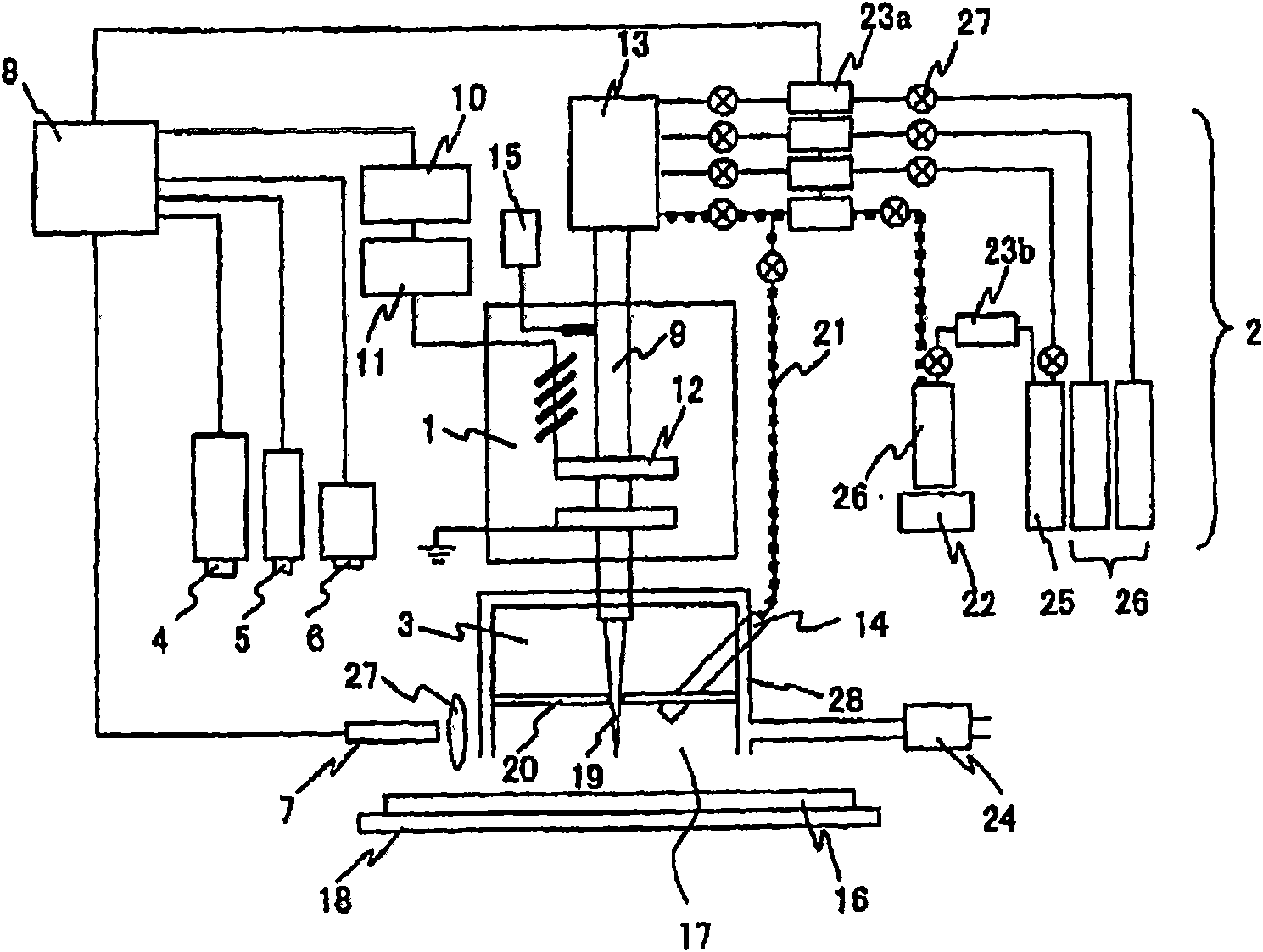
[0066] figure 1 It is a schematic diagram showing a device for repairing the liquid crystal display device (hereinafter sometimes referred to as a repairing device) as Embodiment 1 of the present invention.
[0067] figure 1 Among them, the correction device is roughly composed of the following parts: a local plasma generation part 1 for correcting defects, a gas supply part 2, a plasma reaction part 3, a laser for microprocessing 4, a coating mechanism 5, and a device for identifying defects. A camera 6, a measuring mechanism 7 and a control unit 8 for monitoring the plasma state.
[0068] In the plasma generation unit 1, a thin tube 9 for plasma generation made of a dielectric such as quartz and an electrode 12 for supplying high-frequency power from a high-frequency power source 10 to the outer peripheral region of the thin tube 9 through a matching network 11 are disposed. And constitute. As a specific example, a quartz tube having an inner diameter of φ1.5 mm and an ou...
Embodiment 2
[0097] Next, as a second embodiment of the present invention, a defect correction method of a liquid crystal display device using the correction device described above will be described.
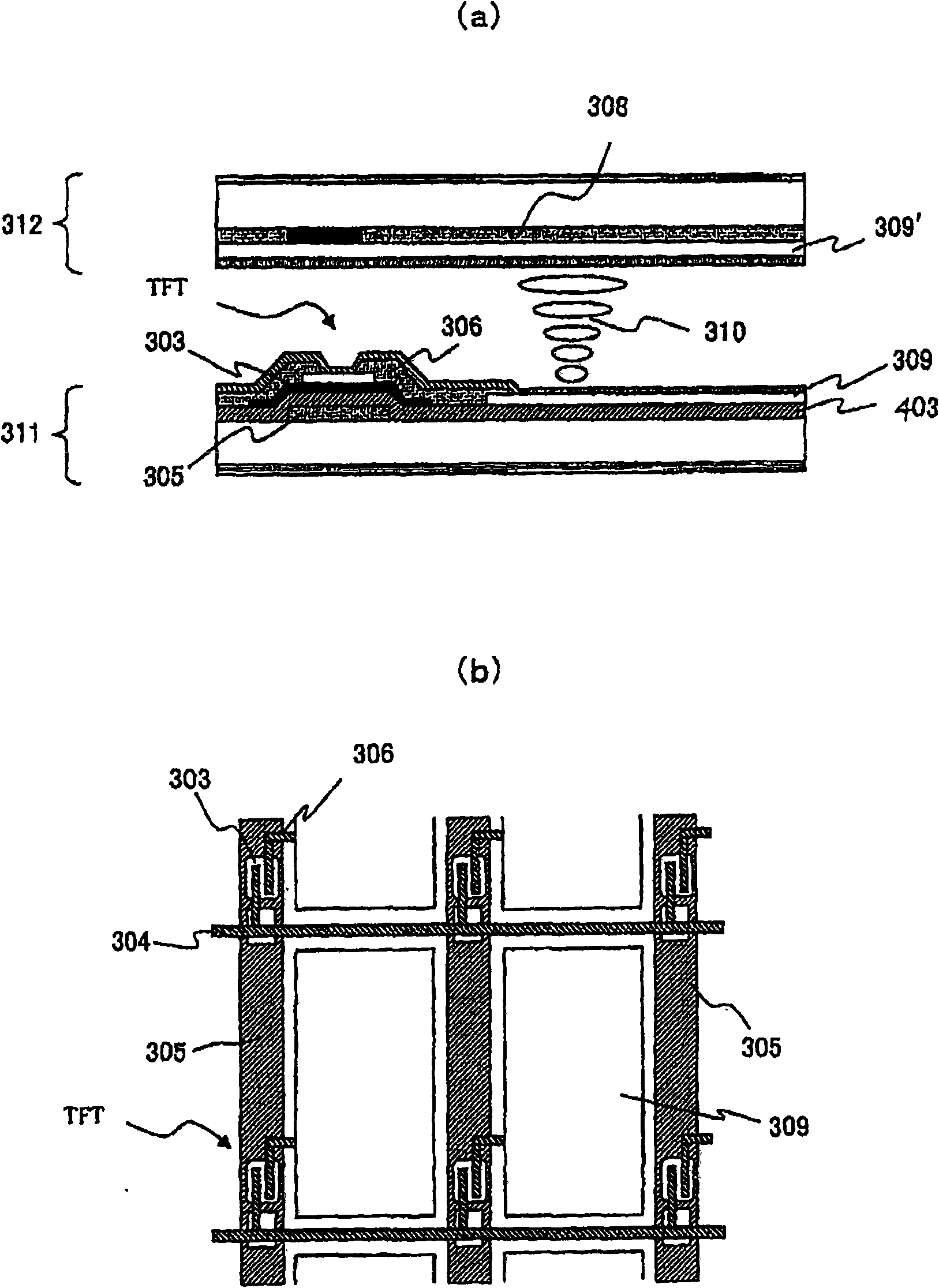
[0098] Here, before describing the defect correction method, use image 3 (a) and (b) schematically illustrate the configuration of a liquid crystal display device to be corrected for defects. image 3 (a) is a sectional view, image 3 (b) is a plan view of a pixel portion.
[0099] exist image 3 In (a), the TFT substrate 311 on which a plurality of pixel portions is formed and the color filter substrate 312 on which a plurality of color filters 308 are formed are arranged such that the pixel portions are opposed to the color filters 308, and there is a gap between them. Liquid crystal 310 is interposed therebetween. Additionally, if image 3 As shown in (b), in the above-mentioned pixel portion, the gate wiring 305 is formed on the TFT substrate 311, and the gate insulating layer 403 ...
Embodiment 3
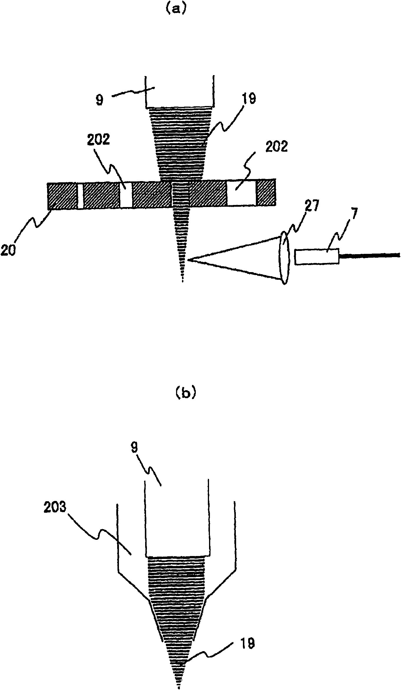
[0131] In Embodiment 3 of the present invention, the correction device has a coating mechanism for applying a resin material such as a photoresist used as a contact mask, and a laser processing device. The processing device has a mechanism capable of performing fine processing of several μm and irradiating laser light in a wide range of several hundred μm.
[0132] The intensity of the plasma irradiated by the above-mentioned plasma jet 19 on the substrate 16 has a Gaussian distribution. Therefore, distribution of film thickness and film quality characteristics occurs from the center to the periphery of the plasma irradiation region, making it difficult to perform microfabrication on the order of μm with high precision. Therefore, a masking process using a resin-based material is used in this embodiment.
[0133] Figure 6 The correction procedure of the disconnection defect part in this contact mask method is shown. Here, with Figure 6 The manufacturing process of the sh...
PUM
| Property | Measurement | Unit |
|---|---|---|
| The inside diameter of | aaaaa | aaaaa |
| Outer diameter | aaaaa | aaaaa |
Abstract
Description
Claims
Application Information