Method for manufacturing CVD silicon oxide capable of improving forming quality

A manufacturing method and technology of forming quality, applied in semiconductor/solid-state device manufacturing, electrical components, circuits, etc., can solve problems such as undercutting is not very serious, photoresist is lifted, affecting the forming effect of CVD silicon oxide, etc. Reduced etch rate, improved adhesion, reduced undercut effect

Inactive Publication Date: 2010-06-02
GRACE SEMICON MFG CORP
View PDF0 Cites 12 Cited by
  • Summary
  • Abstract
  • Description
  • Claims
  • Application Information

AI Technical Summary

Problems solved by technology

The undercut of thermally oxidized silicon oxide is not very serious due to its relatively dense texture, while the texture of CVD silicon oxide is relatively loose, and the u

Method used


Image

  • Method for manufacturing CVD silicon oxide capable of improving forming quality
  • Method for manufacturing CVD silicon oxide capable of improving forming quality
  • Method for manufacturing CVD silicon oxide capable of improving forming quality

Examples


Embodiment Construction

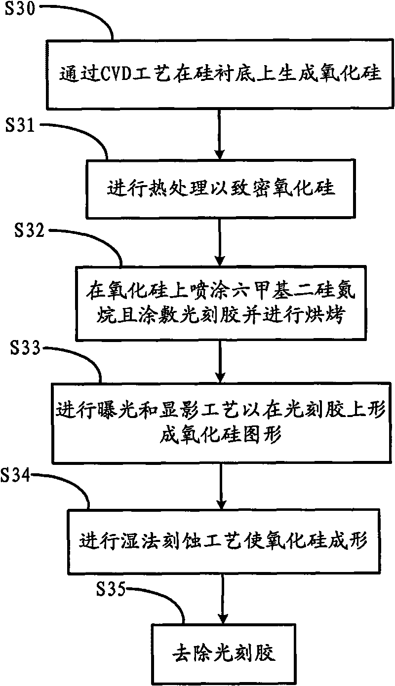
[0022] The CVD silicon oxide manufacturing method capable of improving forming quality of the present invention will be further described in detail below.

[0023] see image 3 , which shows the process flow of the CVD silicon oxide manufacturing method that can improve the forming quality of the present invention. As shown in the figure, the CVD silicon oxide manufacturing method that can improve the forming quality of the present invention first performs step S30, and the silicon substrate is formed by the CVD process. Silicon oxide is formed on the surface, and the CVD process is a low pressure chemical vapor deposition (LPCVD) process or an atmospheric pressure chemical vapor deposition (APCVD) process. In this embodiment, the CVD process is LPCVD.

[0024] Then continue to step S31, and perform heat treatment to densify silicon oxide. To improve efficiency, the heat treatment usually adopts rapid thermal processing (RTP). The processing temperature ranges from 800 to 900...


PUM


Abstract

The invention provides a method for manufacturing CVD silicon oxide capable of improving forming quality. In the prior art, the CVD silicon oxide is not subjected to thermal treatment for compacting before photoetching and etching processes to cause peeling off of photoresist and serious undercut of the CVD silicon oxide due to small adherence force of the silicon oxide with the photoresist. The method comprises the following steps: firstly, growing the silicon oxide on a silicon substrate through a CVD process; secondly, performing thermal treatment on the silicon oxide to compact the silicon oxide; thirdly, coating the photoresist on the silicon oxide, and carrying out exposure and developing processes to form a graph of the silicon oxide on the photoresist; fourthly, carrying out wet etching process to form the silicon oxide; and finally, removing the photoresist. The method can improve the adherence force between the CVD silicon oxide and the photoreist, and reduce the diffusion velocity of etching fluid between interfaces, thereby reducing the etching velocity of the CVD silicon oxide surface, effectively reducing undercut, and effectively improving the forming quality.

Description

technical field [0001] The invention relates to the field of semiconductor manufacturing, in particular to a CVD silicon oxide manufacturing method capable of improving forming quality. Background technique [0002] Silicon oxide is one of the most widely used insulating dielectrics in the field of semiconductor manufacturing. It can be used as field oxide layer, gate oxide layer and shallow trench isolation structure (STI), etc. Silicon oxide can be produced by thermal oxidation and chemical vapor deposition. (Chemical Vapor Deposition; CVD for short) process, and the silicon oxide produced by it is referred to as thermal oxide silicon oxide and CVD silicon oxide for short. [0003] In the field of semiconductor manufacturing, dilute hydrofluoric acid (Dilute HF; referred to as DHF) or hydrofluoric acid buffered etching solution (Buffered HF; referred to as BHF) is usually used to etch the above-mentioned thermally oxidized silicon oxide and CVD silicon oxide, and the etche...

Claims


Application Information

Patent Timeline
IPC IPC(8): H01L21/316H01L21/3105
Inventor 郭国超
Owner GRACE SEMICON MFG CORP
Why Eureka
Try Eureka