Method for preparing semicylindrical minute groove by utilizing secondary film deposition and wet etching
A wet etching, semi-cylindrical technology, applied in the manufacture of microstructure devices, processes for producing decorative surface effects, coatings, etc., can solve the problem that the processing area is only on the order of microns and the cost is expensive, and achieve high efficiency Processing route, effect of reducing preparation cost
- Summary
- Abstract
- Description
- Claims
- Application Information
AI Technical Summary
Problems solved by technology
Method used
Image

Examples
Embodiment 1
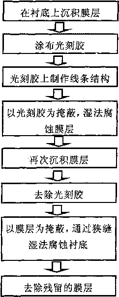
[0025] Embodiment 1, making the semi-cylindrical fine groove of diameter 1 micron, making process such as figure 1 As shown, the details are as follows:
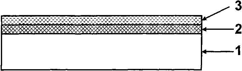
[0026] (1) Select a quartz plate with a thickness of 360 microns as the substrate; use magnetron sputtering technology to deposit a layer of 100 nanometers thick metal chromium layer on the surface of the substrate, and coat AR-P3100 with a thickness of 1.1 microns on the chromium layer Photoresist (such as figure 2 shown).
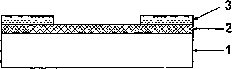
[0027] (2) Through exposure, development, hard mold, prepare such as image 3 The line structure shown.
[0028] (3) if Figure 4 As shown, using the photoresist pattern as a mask and the isotropic characteristics of wet etching, the metal chromium layer below the edge of the photoresist line pattern is etched away by using an etching solution. The corrosion solution is a chrome removal solution, its proportion is 100ml of water, 13ml of perchloric acid, 50g of tetraammonium nitrate, the corrosion...
Embodiment 2
[0031] Embodiment 2 makes the semi-cylindrical micro-grooves with a diameter of 700 nanometers, and the manufacturing process is as follows figure 1 As shown, the details are as follows:
[0032] (1) Select a quartz plate with a thickness of 1000 microns as the substrate; use magnetron sputtering technology to deposit a layer of 50 nanometers thick metal chromium layer on the surface of the substrate, and coat AR-P3100 with a thickness of 1.1 microns on the chromium film Photoresist (such as figure 2 shown).
[0033] (2) Through exposure, development, hard mold, prepare such as image 3 The line structure shown.
[0034] (3) if Figure 4 As shown, using the photoresist pattern as a mask and the isotropic characteristics of wet etching, the metal chromium layer below the edge of the photoresist line pattern is etched away by using an etching solution. The corrosion solution is a chrome removal solution, the proportion of which is 100ml of water, 13ml of perchloric acid, 5...
Embodiment 3
[0037] Embodiment 3 makes the semi-cylindrical fine groove of diameter 2 microns, and manufacturing process is as follows figure 1 As shown, the details are as follows:
[0038] (1) Select a quartz plate with a thickness of 1000 microns as the substrate; use magnetron sputtering technology to deposit a layer of 150 nanometers thick metal chromium layer on the surface of the substrate, and coat AR-P3100 with a thickness of 1.1 microns on the chromium film Photoresist (such as figure 2 shown).
[0039] (2) Through exposure, development, hard mold, prepare such as image 3 The line structure shown.
[0040] (3) if Figure 4As shown, using the photoresist pattern as a mask and the isotropic characteristics of wet etching, the metal chromium layer below the edge of the photoresist line pattern is etched away by using an etching solution. The corrosion solution is a chrome removal solution, its proportion is 100ml of water, 13ml of perchloric acid, 50g of tetraammonium nitrate...
PUM
| Property | Measurement | Unit |
|---|---|---|
| Thickness | aaaaa | aaaaa |
| Thickness | aaaaa | aaaaa |
| Thickness | aaaaa | aaaaa |
Abstract
Description
Claims
Application Information
 - R&D
- Intellectual Property
- Life Sciences
- Materials
- Tech Scout
- Unparalleled Data Quality
- Higher Quality Content
- 60% Fewer Hallucinations
Browse by: Latest US Patents, China's latest patents, Technical Efficacy Thesaurus, Application Domain, Technology Topic, Popular Technical Reports.
© 2025 PatSnap. All rights reserved.Legal|Privacy policy|Modern Slavery Act Transparency Statement|Sitemap|About US| Contact US: help@patsnap.com