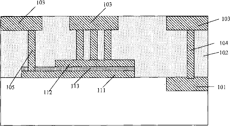
Formation method of silicon oxide film and metal-insulator-metal capacitor
A silicon oxide and thin film technology, applied in metal material coating process, circuits, electrical components, etc., can solve the problems of poor dynamic characteristics of MIM capacitors, improve dynamic characteristics, stabilize capacitance voltage coefficient and capacitance temperature coefficient, and stabilize electric capacity. performance effect
- Summary
- Abstract
- Description
- Claims
- Application Information
AI Technical Summary
Problems solved by technology
Method used
Image
Examples
no. 1 example
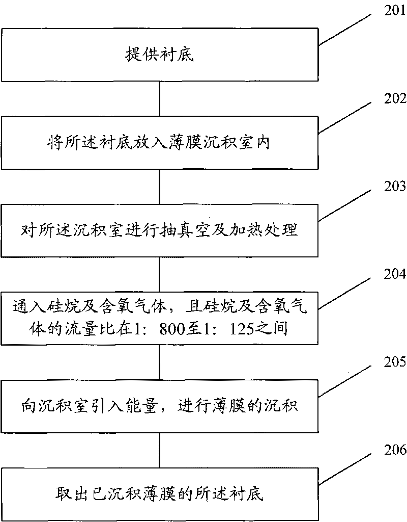
[0066] The first embodiment of the present invention introduces a new method for forming a silicon oxide film, figure 2 for
[0067] The flowchart of the method for forming a silicon oxide film according to the first embodiment of the present invention is combined below figure 2 The first embodiment of the present invention will be described in detail.
[0068] Step 201: providing a substrate.
[0069] The substrate provided in this embodiment may be a simple silicon substrate, or a silicon substrate on which metal oxide semiconductor transistors have been formed, or a substrate on which an underlying metal wiring structure has been formed.
[0070] In other embodiments of the present invention, semiconductor substrates of other materials may also be used, such as germanium substrates, gallium arsenide substrates, and the like.
[0071] Step 202: Put the substrate into a film deposition chamber.
[0072] The film deposition equipment used in this embodiment is PECVD. In ...
no. 2 example
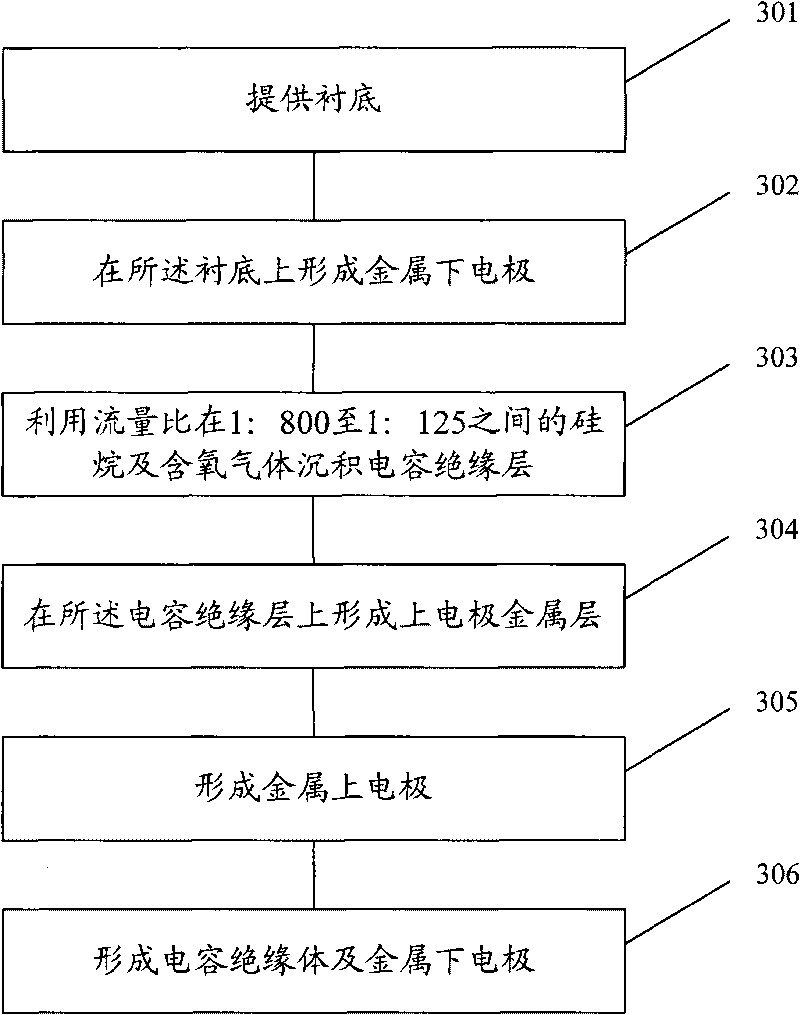
[0090] The second embodiment of the present invention introduces a new method for forming a MIM capacitor, image 3 It is a flowchart of a method for forming a MIM capacitor according to the second embodiment of the present invention, Figure 4 to Figure 10 In order to illustrate the schematic cross-sectional view of the device of the MIM capacitance forming method of the second embodiment of the present invention, the following is combined Figure 3 to Figure 10 The second embodiment of the present invention will be described in detail.
[0091] Step 301: Provide a substrate.
[0092] The substrate provided in this embodiment may be a silicon substrate on which a metal oxide semiconductor transistor has been formed, or a substrate on which an underlying metal wiring structure has been formed.
[0093] Figure 4 is a schematic cross-sectional view of the substrate provided in the second embodiment of the present invention, such as Figure 4 As shown, the underlying conduct...
PUM
 Abstract
Description
Claims
Application Information


