Method for manufacturing integrated PNP differential pair tube

A manufacturing method and technology of differential pair tubes, which are applied in the manufacture of semiconductor/solid-state devices, electrical components, circuits, etc., can solve the problems of low reverse amplification factor, good symmetry of differential pair tubes, and high frequency, and reduce the saturation voltage drop. , the effect of high reliability

Inactive Publication Date: 2011-07-20
JINZHOU 777 MICROELECTRONICS
View PDF0 Cites 0 Cited by
  • Summary
  • Abstract
  • Description
  • Claims
  • Application Information

AI Technical Summary

Problems solved by technology

[0002] Due to the good symmetry and high frequency of ordinary differential pair tubes, which are much larger than several hundred megahertz, they can be used in the input poles and preamplifiers of instruments and instruments, but their base-emitter reverse breakdown voltage wears a relatively large range of BVcbo. Low, generally 5 ~ 12V, and the reverse amplification factor is very low, close to zero
Therefore, ordinary differential pair tubes are not suitable for some applications that need to withstand high voltage without damage and require a large reverse DC amplification factor β

Method used


Image

  • Method for manufacturing integrated PNP differential pair tube
  • Method for manufacturing integrated PNP differential pair tube
  • Method for manufacturing integrated PNP differential pair tube

Examples


Embodiment 1

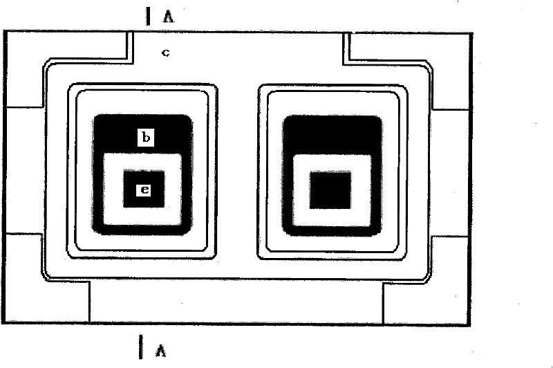
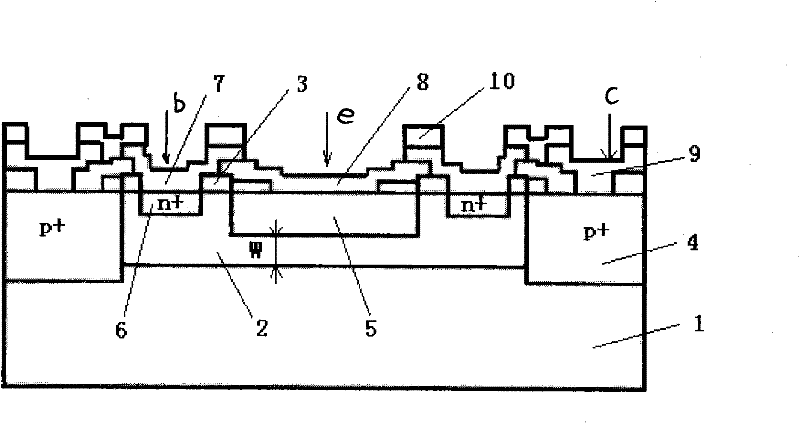
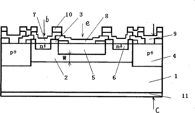
[0018] 1. If figure 1 with figure 2 As shown, the single-sided polished P+ silicon substrate 1 with crystal orientation has a resistivity of 0.001 ohm-cm, and an epitaxial layer is grown on the silicon substrate 1 as the N-base region 2, and the resistivity is 0.2 ohm-cm , with a thickness of 20 μm, an oxide layer 3 is grown by thermal oxidation;

[0019] 2. Diffusion of boron on the surface of the N base region 2 by photolithographic masking and etching, and the temperature of re-diffusion is 1160°C. The diffused boron junction is connected to the P+ silicon substrate 1 as the common P+ collector region 4 and forms a protective ring, and the epitaxial layer is separated into Two independent base regions, the surface impurity concentration of P+ collector region 4 is 10 20 / cm 3 ;

[0020] 3. Diffuse boron on the surface of the N-base region 2 to form a discrete emission region 5 through photolithographic masking and etching, and then diffuse at a temperature of 1000°C, ...

Embodiment 2

[0024] 1. If figure 1 with figure 2 As shown, the crystal direction is selected to polish the P+ silicon substrate 1 on one side, and its resistivity is 0.008 ohm-cm. An epitaxial layer is grown on the silicon substrate 1 as the N base region 2, and the resistivity is 2.0 ohm-cm. The thickness is 10 μm, and a layer of oxide layer 3 is grown by thermal oxidation;

[0025] 2. Diffusion of boron on the surface of the N base region 2 by photolithographic masking and etching, and the temperature of re-diffusion is 1200°C. The diffused boron junction is connected to the P+ silicon substrate 1 as the common P+ collector region 4 and forms a guard ring, and the epitaxial layer is separated into Two independent base regions, the surface impurity concentration of P+ collector region 4 is 4×10 19 / cm 3 ;

[0026] 3. Diffuse boron on the surface of the N-base region 3 to form the emitter region 5 by photolithographic masking and etching, and then diffuse at a temperature of 1160°C, ...

Embodiment 3

[0030] 1. If figure 1 with figure 2 As shown, the crystal direction is selected to polish the P+ silicon substrate 1 on one side, and its resistivity is 0.005 ohm-cm. An epitaxial layer is grown on the silicon substrate 1 as the N base region 2, and the resistivity is 1.0 ohm-cm. The thickness is 15 μm, and a layer of oxide layer 3 is grown by thermal oxidation;

[0031] 2. Diffuse boron on the surface of the N-base region 2 through photolithographic masking and etching, and the temperature of the re-diffusion is 1190°C. The diffused boron junction is connected to the P+ silicon substrate 1 as the common P+ collector region 4 and forms a guard ring, and the epitaxial layer is separated into Two independent base regions, the surface impurity concentration of P+ collector region 4 is 6×10 19 / cm 3 ;

[0032] 3. Diffuse boron on the surface of the N-base region 3 to form the emission region 5 by photolithographic masking and etching, and then diffuse at a temperature of 103...


PUM

PropertyMeasurementUnit
thicknessaaaaaaaaaa
thicknessaaaaaaaaaa
thicknessaaaaaaaaaa

Abstract

The invention relates to a method for manufacturing an integrated PNP differential pair tube. The method comprises the following steps: selecting a one-side polishing P+ silicon substrate with specific resistance ranging between 0.001 and 0.008ohm-centimeter; growing an epitaxial layer serving as an N base region on the silicon substrate, wherein the specific resistance of the epitaxial layer is between 0.2 and 2.0ohm-centimeter and the thickness is between 10 and 20 mu m, and growing an oxidation layer through thermal oxidation; diffusing boron on the surface of the N base region and connecting a diffused boron agglomeration with the P+ silicon substrate to form a common P+ collecting zone, and separating the epitaxial layer into two separate base regions; diffusing the boron on the surface of the N base region to form an emitter region and controlling the effective width of the N base region between 5 and 10 mu m; diffusing phosphorus on the surface of the N base region to form a contact zone of the N+ base region; leading metal electrodes out from the surface of the contact zone of the N+ base region, the P+ collecting zone surface and the emitter region surface; and leading the metal electrodes out from the surface of the P+ collecting zone or the back side of the P+ silicon substrate. The method has the advantages that the method can effectively reduce saturation voltage drop to ensure that base-emitter reverse voltage reaches 30-100V; and devices not only have a large forward DC amplification coefficient Beta, but also have a reverse DC amplification coefficient Betareaching 8 to 15.

Description

technical field [0001] The invention relates to a manufacturing method of an integrated PNP differential pair tube. Background technique [0002] Due to the good symmetry and high frequency of ordinary differential pair tubes, which are much larger than several hundred megahertz, they can be used in the input poles and preamplifiers of instruments and instruments, but their base-emitter reverse breakdown voltage wears a relatively large range of BVcbo. Low, generally 5 ~ 12V, and the reverse amplification factor is very low, close to zero. Therefore, ordinary differential pair tubes are not suitable for some applications that need to withstand high voltage without damage and require a large reverse DC amplification factor β. Contents of the invention [0003] The technical problem to be solved by the present invention is to provide a manufacturing method of an integrated PNP differential pair tube, the base-emitter reverse voltage is high, the reverse amplification factor...

Claims


Application Information

Patent Timeline
Patent Type & Authority Patents(China)
IPC IPC(8): H01L21/331
Inventor 张小平邱晓华罗志勇李书艳刘芝连
Owner JINZHOU 777 MICROELECTRONICS
Why Eureka
Try Eureka