Nano-wire field effect transistor
A field effect transistor, transistor technology, applied in semiconductor devices, electrical components, circuits, etc., to reduce off-state current, increase current switching ratio, and improve performance.
- Summary
- Abstract
- Description
- Claims
- Application Information
AI Technical Summary
Problems solved by technology
Method used
Image
Examples
Embodiment 1
[0019] Embodiment 1. Silicon nanowire field effect transistor with core-shell structure and its performance testing
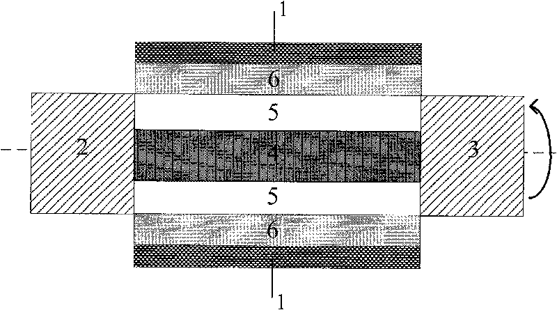
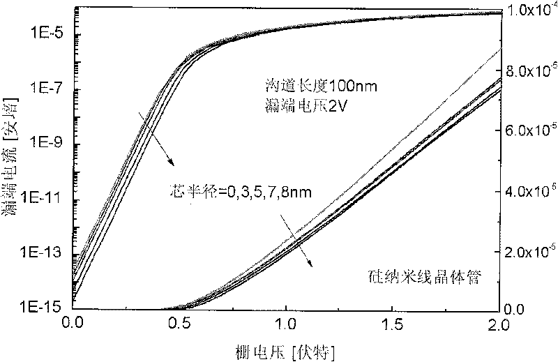
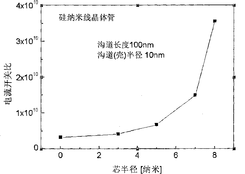
[0020] The structure of the nanowire field effect transistor is as follows figure 1 As shown, where the work function of the gate electrode 1 material is set to 4.61 electron volts, the source region 2 and the drain region 3 are doped with phosphorus at a concentration of 1×10 20 cm -3 silicon material, the core part 4 is silicon oxide, and the shell part 5 is boron doping concentration 1×10 11 cm -3 silicon material, and the gate dielectric layer 6 is silicon oxide with a thickness of 2nm. The shell radius of the core-shell structure is 10 nm, the length of the core-shell structure is 0.1 micron, and the core radius is adjustable.
[0021] The above-mentioned transistors can be prepared according to existing methods, and the preparation process is briefly described as follows:
[0022] 1) Etch the silicon pillars on the silicon wafer with a circular silic...
Embodiment 2
[0031] Embodiment 2, germanium nanowire field effect transistor with core-shell structure and its performance detection
[0032] The structure of the nanowire field effect transistor is still as figure 1 As shown, wherein, the work function of the gate electrode 1 material is set to 4.33 electron volts, the source region 2 and the drain region 3 are doped with arsenic concentration of 1×10 20 cm -3 germanium, the core part 4 is silicon oxide, and the shell part 5 is boron doping concentration 2×10 12 cm -3 germanium material, and the gate dielectric layer 6 is silicon oxide with a thickness of 1.5nm. The shell radius of the core-shell structure is set at 10 nm, the length of the core-shell structure is 100 nm, and the core radius is adjustable.
[0033] The current output characteristics, switching ratio, threshold voltage and leakage-induced barrier lowering effect of the transistor device were tested respectively, and the results obtained are as follows: Figure 6-Figur...
PUM
 Abstract
Description
Claims
Application Information


