Annealed wafer and method for producing annealed wafer

An annealing and wafer technology, applied in chemical instruments and methods, crystal growth, single crystal growth, etc., can solve problems such as weak Cu gettering effect, weak gettering effect, and poor device reliability

Inactive Publication Date: 2010-06-23
SILTRONIC AG
View PDF0 Cites 14 Cited by
  • Summary
  • Abstract
  • Description
  • Claims
  • Application Information

AI Technical Summary

Problems solved by technology

[0006] However, according to the report of Non-Patent Document 1, such as figure 1 As shown, it has been pointed out that even the IG material has a weak gettering effect on Cu (wiring material for high rate devices), and has a problem of deterioration of device reliability due to the fact that even at a low temperature (about 400°C) Cu pollution caused by re-emission of Cu absorbed (trapped) by heat treatment (such as wiring step) in the device process
However, even in a wafer obtained by performing 3-stage heat treatment on a general DZ-IG wafer, there is a problem that the gettering effect on Cu is weak, and thus there is a problem that the reliability of the device is deteriorated due to Cu contamination, the Cu contamination is caused by the re-emission of Cu absorbed (trapped) by thermal processing (such as wiring steps) in the device process even at low temperature (about 400°C)

Method used


Image

  • Annealed wafer and method for producing annealed wafer
  • Annealed wafer and method for producing annealed wafer
  • Annealed wafer and method for producing annealed wafer

Examples


Embodiment 1

[0066] By using the CZ method, the nitrogen concentration was pulled up to 3 x 10 15 / cm 3 (measured by SIMS), the carbon concentration is 8×10 15 / cm 3 , and the oxygen concentration is 9×10 17 / cm 3 Silicon single crystal (measured by FT-IR according to JEIDA standard).

[0067] After slicing and polishing the resulting silicon single crystal to obtain mirror wafers (silicon substrates), during the manufacturing process, the mirror wafers were inserted into a furnace at 700 °C under an atmosphere containing nitrogen and oxygen, specifically, nitrogen-based, oxygen-containing The mirror wafer was heat-treated at 700°C for 4 hours in an atmosphere having a concentration of 0.2% by volume, and then pulled out from the furnace.

[0068] Then, the oxide film of the silicon substrate under heat treatment is removed by etching, and the silicon substrate is inserted into a furnace under an argon atmosphere, specifically, 100% argon gas. After heating it from 700°C to 1000°C at...

Embodiment 2

[0072] By using the CZ method, the nitrogen concentration was pulled up to 2 x 10 15 / cm 3 (measured by SIMS), the carbon concentration is 8×10 15 / cm 3 , and the oxygen concentration is 9×10 17 / cm 3 Silicon single crystal (measured by FT-IR according to JEIDA standard).

[0073] After slicing and polishing the resulting silicon single crystal to obtain a mirror wafer (silicon substrate), during the manufacturing process, the mirror wafer is inserted into a furnace at 700°C under an argon atmosphere with an argon concentration of 100%, and the mirror wafer is kept in the furnace 4 hours. Then, it was annealed with argon at 1200° C. for 1 hour by raising the temperature to 1000° C. at a rate of 8° C. / min., and then raising the temperature to 1100° C. at a rate of 4° C. / min. °C, and raised to 1200 °C at a rate of 1 °C / min to pull out the silicon substrate from the furnace.

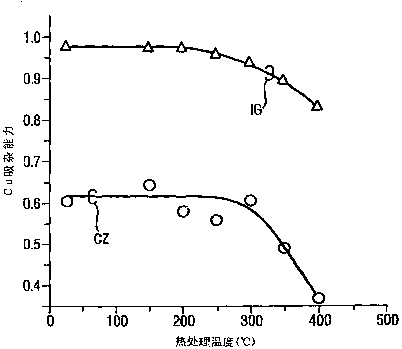
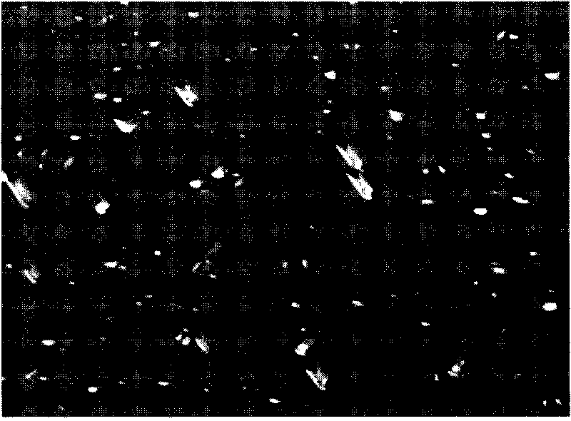
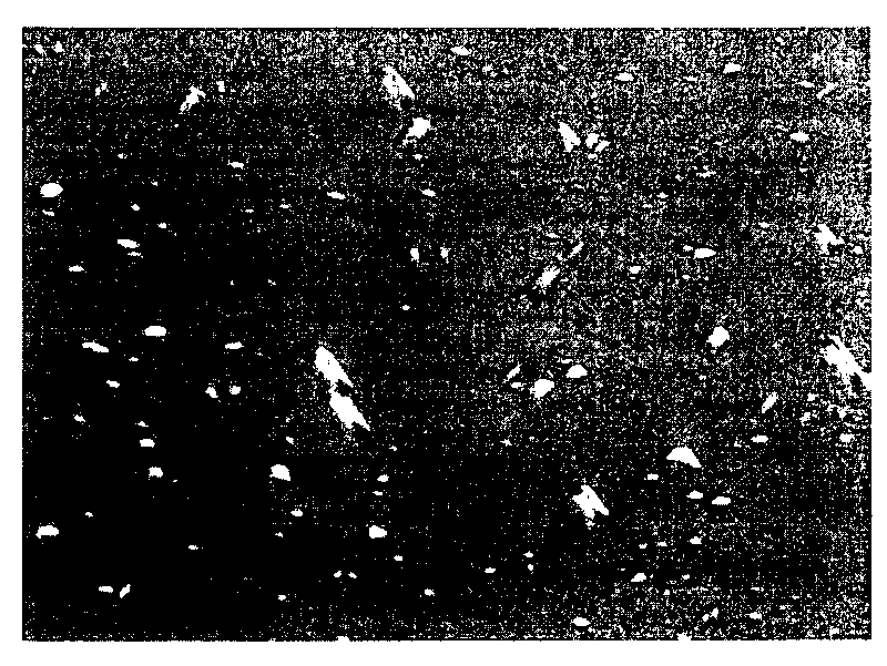
[0074] Observing the internal oxygen deposits after annealing with a transmission electron micros...


PUM

PropertyMeasurementUnit
sizeaaaaaaaaaa
sizeaaaaaaaaaa
sizeaaaaaaaaaa

Abstract

An annealed wafer having enhanced gettering effects for Cu is produced by heating a silicon substrate containing a nitrogen concentration of 5X10¹⁴ to 1X10¹⁶ / cm3, a carbon concentration of 1X10¹⁵ to 5X10¹⁶ / cm3, and an oxygen concentration of 6X10¹⁷ to 11X1017 / cm3 at a temperature of 650 to 800 DEG C. for a time >=4 hours, and subjecting the heated substrate to argon annealing at a temperature of 1100 to 1250 DEG C., wherein internal stacking fault density after annealing is >=5X10⁸ / cm3.

Description

technical field [0001] The present invention relates to annealed wafers and methods of making annealed wafers. Background technique [0002] Semiconductor substrates, especially silicon single wafers (hereinafter also simply referred to as substrates) have been used as substrates for the fabrication of highly integrated MOS devices. Most silicon single wafers are substrates cut from silicon single crystal ingots manufactured by the Czochralski (CZ) method. [0003] In such a silicon single wafer, the oxygen introduced during the preparation of the single crystal exists in a supersaturated state, which will be deposited in the subsequent device process to form oxygen precipitates (oxygenprecipitates) in the substrate (deposition of silicon oxide Generally known as BMD: Bulk Micro Defect). It is known that the generation of oxygen deposits in the active region of the device is a factor for the deterioration of device characteristics (such as a decrease in the withstand volta...

Claims


Application Information

Patent Timeline
Patent Type & Authority Applications(China)
IPC IPC(8): C30B33/02
CPCC30B33/02C30B29/06C30B15/02H01L21/322H01L21/324
Inventor 石坂和纪中居克彦福田真行
Owner SILTRONIC AG
Why Eureka
Try Eureka