Positive pressure thermoforming manufacturing method of wafer-level glass micro-channel

A manufacturing method and glass micro technology, which are applied in the manufacture of microstructure devices, microstructure technology, microstructure devices, etc., can solve the problems of high cost, uncontrollable shape of microchannels, shallow channels, etc., and achieve low cost and molding. The effect of high height and simple method

Active Publication Date: 2010-06-30
SOUTHEAST UNIV
View PDF0 Cites 6 Cited by
  • Summary
  • Abstract
  • Description
  • Claims
  • Application Information

AI Technical Summary

Problems solved by technology

This method requires vacuum conditions, and usually requires special bonding equipment with vacuum, so the cost is high; in addition, this method uses negative pressure forming, so the formed micro-channels are located on the back of the glass wafer, so the glass When the wafer is thicker, the shape of the microchannel formed on the back is uncontrollable and the channel is shallow; when forming a taller glass microchannel, it is usually necessary to use a thicker silicon wafer and etch a deep silicon cavity (Some even need to reach 900 microns, Glass Blowing on a WaferLevel, JOURNAL OF MICROELECTROMECHANICAL SYSTEMS, VOL.16, NO.2, APRIL2007) and a high aspect ratio to provide enough gas, so that the glass bubbles are fully formed, with a relatively high High height to form a higher arc; sometimes it is even necessary to etch a larger hole on another silicon wafer, and then bond with the silicon wafer with a through hole, so as to provide enough gas to form a higher height , glass microchannels with better curvature usually cost more

Method used


Image

  • Positive pressure thermoforming manufacturing method of wafer-level glass micro-channel
  • Positive pressure thermoforming manufacturing method of wafer-level glass micro-channel
  • Positive pressure thermoforming manufacturing method of wafer-level glass micro-channel

Examples


Embodiment 1

[0027] A positive pressure thermoforming manufacturing method for a wafer-level glass microchannel, comprising the following steps:

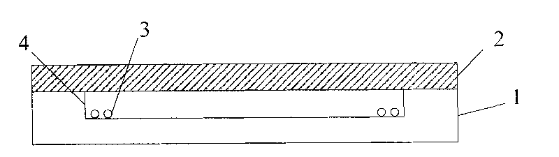
[0028] The first step is to use the Si micromachining process to etch the microfluidic shallow groove pattern on the Si wafer (such as a 4-inch wafer). The silicon wafer used can be a silicon wafer with a standard thickness, such as a 500 micron thick silicon wafer. The depth of the shallow groove is 10-200 microns, such as 15 microns, 30 microns, 40 microns, 60 microns, 95 microns, 132 microns, 150 microns, 180 microns, and the aspect ratio is usually less than 2, such as 1.5, 1, 0.8, 0.5, 0.2, 0.1, 0.05, 0.02, the micromachining process of the pattern structure on the Si wafer is a wet etching process, or a dry inductively coupled plasma (ICP) etching process, reactive ion etching One of them, preferably a wet etching process (lower cost), such as etching with a TMAH solution, the pattern can be striped or serpentine, and can be adjusted as ne...

Embodiment 2

[0035] A positive pressure thermoforming manufacturing method for a wafer-level glass microchannel, comprising the following steps:

[0036] The first step is to use Si micromachining technology to etch microchannel shallow grooves on a 4-inch Si wafer. The silicon wafer used can be a silicon wafer with a standard thickness and a thickness of 500 microns. The depth of the shallow grooves is 60 microns. The runner groove is a strip groove with a diameter of 2 mm, and the length of the groove is 3 cm. The micromachining process of the pattern structure on the Si wafer is a wet etching process, and the used etching solution is a TMAH solution with a concentration of 10% and a temperature of 80 degrees Celsius,

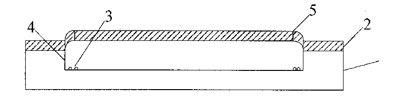
[0037] In the second step, chemically pure calcium carbonate powder is placed in a shallow tank with a particle size of 5 microns and a mass of 30 micrograms.

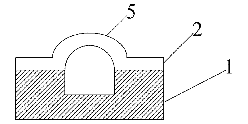
[0038] The 3rd step, above-mentioned Si disc and Pyrex7740 glass disc (a kind of brand of borosilicate glass, ...

Embodiment 3

[0042] A positive pressure thermoforming manufacturing method for a wafer-level glass microchannel, comprising the following steps:

[0043] The first step is to use Si micromachining technology to etch microchannel shallow grooves on a 4-inch Si wafer. The silicon wafer used can be a silicon wafer with a standard thickness and a thickness of 500 microns. The depth of the shallow grooves is 100 microns. The groove is a strip-shaped groove with a diameter of 1 mm and a length of 2 cm. The micromachining process of the pattern structure on the Si wafer is a wet etching process. The etching solution used is a TMAH solution with a concentration of 10% and a temperature of 80 degrees Celsius. ,

[0044] In the second step, titanium hydride is placed in a shallow tank, the powder particle size is 5 microns, and the mass is 25 micrograms. The high-temperature air release agent can also be preferably pretreated titanium hydride, and the titanium hydride is pretreated in the air at 400...


PUM


Abstract

The invention discloses a positive pressure thermoforming manufacturing method of a wafer-level glass micro-channel, which comprises the following steps of: 1. etching a specific silicon micro-channel shallow slot pattern on a Si wafer by utilizing a Si microprocessing process; 2. locally placing a proper amount of high-temperature gas releasing agent at both ends or a specific position of a silicon micro-channel; 3. bonding the Si wafer and a Pyrex7740 glass wafer to enable a shallow slot on Pyrex7740 glass to form a sealed cavity body; and 4. heating the bonded wafers to the temperature of 810-890 DEG C in air, preserving heat for 5-10 minutes, releasing gas by the high-temperature gas releasing agent due to heating, generating a positive pressure to enable molten glass corresponding to the sealed cavity body to deform and form a micro-channel pattern corresponding to the silicon micro-channel shallow slot pattern on the glass, and cooling to obtain the wafer-level glass micro-channel. In the invention, the gas is released by utilizing the high-temperature gas releasing agent, so that the glass can be in the shape of a hemispherical arc pipe to form the glass micro-channel.

Description

technical field [0001] The invention relates to a microsystem manufacturing technology, in particular to a positive pressure thermoforming manufacturing method of a wafer-level glass micro flow channel. Background technique [0002] In the field of MEMS manufacturing technology, Pyrex7740 glass (a glass containing alkaline ions, Pyrex is Corning's product brand) is an important material. It has a thermal expansion coefficient similar to that of Si materials, and has high light transmittance. High strength, and can form a high-strength bonding connection with the Si substrate by using the anodic bonding process, and a strong Si-O covalent bond is generated on the bonding surface, and its strength is even higher than that of the Si material itself. Due to such characteristics, Pyrex7740 glass is widely used in MEMS packaging, microfluidics and MOEMS (micro-optical electro-mechanical systems) and other fields. [0003] At present, the microfluidic system is mainly used in the ...

Claims


Application Information

Patent Timeline
Patent Type & Authority Applications(China)
IPC IPC(8): B81C1/00
Inventor 尚金堂陈波寅张迪徐超柳俊文唐洁影黄庆安
Owner SOUTHEAST UNIV
Why Eureka
Try Eureka