Quantum well epitaxy structure of semiconductor laser in 940 nm-1000 nm wave band

An epitaxial structure and semiconductor technology, applied in the direction of semiconductor lasers, lasers, laser components, etc., can solve the problems of low photoelectric conversion efficiency and high operating voltage of semiconductor lasers

Inactive Publication Date: 2010-06-30
THE 13TH RES INST OF CHINA ELECTRONICS TECH GRP CORP
View PDF0 Cites 12 Cited by
  • Summary
  • Abstract
  • Description
  • Claims
  • Application Information

AI Technical Summary

Problems solved by technology

[0005] The technical problem to be solved by the present invention is to provide a semiconductor laser quantum well epitaxial structure in the 940nm-1000nm band. The problem of low conversion efficiency

Method used


Image

  • Quantum well epitaxy structure of semiconductor laser in 940 nm-1000 nm wave band
  • Quantum well epitaxy structure of semiconductor laser in 940 nm-1000 nm wave band
  • Quantum well epitaxy structure of semiconductor laser in 940 nm-1000 nm wave band

Examples


Embodiment Construction

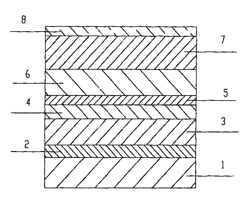
[0013] refer to figure 1 The semiconductor laser quantum well epitaxy structure in the 940nm~1000nm band provided by the present invention comprises: a substrate 1, a buffer layer 2 deposited on the substrate 1 in sequence, a lower confinement layer 3, a lower waveguide layer 4, a quantum well layer 5, an upper waveguide Layer 6, upper confinement layer 7, electrode contact layer 8, wherein: the upper waveguide layer 6 and the lower waveguide layer 4 are Al x GaAs, x=0.13~0.2; upper confinement layer 7 and lower confinement layer 3 are Al y GaAs, y=0.3-0.39.

[0014] Substrate 1: Substrate 1 is used to carry out the epitaxial growth of each layer of semiconductor laser material thereon. In the present invention, substrate 1 is N-type gallium arsenide of (100) plane, which can facilitate the injection of electrons and reduce the thickness of the substrate. Series resistance of bottom 1 material.

[0015] Buffer layer 2: The buffer layer 2 is made on the substrate 1 and is an...


PUM


Abstract

The invention discloses a quantum well epitaxy structure of a semiconductor laser, in particular to a quantum well epitaxy structure of a high-efficiency semiconductor laser in a 940 nm-1000 nm wave band. The quantum well epitaxy structure comprises a substrate, a buffer layer, a lower limiting layer, a lower waveguide layer, a quantum well layer, an upper waveguide layer, an upper limiting layer and an electrode contact layer, wherein the buffer layer, the lower limiting layer, the lower waveguide layer, the quantum well layer, the upper waveguide layer, the upper limiting layer and the electrode contact layer are sequentially deposited on the substrate; the upper waveguide layer and the lower waveguide layer are AlxGaAs, and x is equal to 0.13-0.2; and the upper limiting layer and the lower limiting layer are AlyGaAs, and y is equal to 0.3-0.39. The quantum well epitaxy structure solves the problems of high working voltage and low photoelectric conversion efficiency of the semiconductor laser by optimizing the Al content of the waveguide layers and the limiting layers of the quantum well epitaxy structure, and achieves the purposes of reducing the working voltage and enhancing the photoelectric conversion efficiency.

Description

technical field [0001] The invention relates to the field of semiconductor lasers, in particular to a quantum well epitaxial structure of a semiconductor laser with low turn-on voltage and high efficiency in the 940nm-1000nm band. Background technique [0002] In recent years, almost all active regions of high-power semiconductor lasers use strained quantum well structures, because the strain effect and quantum size effect reduce the effective mass and density of states in the valence band of semiconductor lasers to obtain lower threshold currents. Density, thereby improving the working characteristics of the laser. Since the development of semiconductor lasers, the threshold current density has been from 1000A / cm 2 Reduced to 100A / cm 2 Next, the wavelength develops from infrared to far-infrared and visible light, and the output power continues to increase. The output power of a single tube develops from hundreds of milliwatts to several watts, and the performance is impro...

Claims


Application Information

Patent Timeline
Patent Type & Authority Applications(China)
IPC IPC(8): H01S5/343
Inventor 陈宏泰林琳车相辉王晶徐会武杨红伟安振峰
Owner THE 13TH RES INST OF CHINA ELECTRONICS TECH GRP CORP
Why Eureka
Try Eureka