BCD device and manufacturing method thereof

A device and the same technology, applied in the field of semiconductor power devices, can solve problems such as high on-resistance, increase in on-resistance, and reduce surface field, and achieve the goal of increasing conductive channels, reducing paths, and reducing on-resistance Effect

Inactive Publication Date: 2010-07-07
UNIV OF ELECTRONICS SCI & TECH OF CHINA
View PDF0 Cites 26 Cited by
  • Summary
  • Abstract
  • Description
  • Claims
  • Application Information

AI Technical Summary

Problems solved by technology

However, due to the Ron∝BV2.3~2.6 relationship between the on-resistance Ron of the DMOS device and the device withstand voltage BV, the on-resistance of the device rises sharply when the device is used in high voltage, which limits the lateral high voltage. Application of DMOS devices in high-voltage power integrated circuits, especially in circuits requiring low conduction loss and small chip area
In order to overcome the problem of high on-resistance, J.A. APPLES and others proposed RESURF (Reduced SURface Field) to reduce the surface field technology, which is widely used in the design of high-voltage devices, but it still cannot effectively solve the problem of high on-resistance

Method used


Image

  • BCD device and manufacturing method thereof
  • BCD device and manufacturing method thereof

Examples


Embodiment Construction

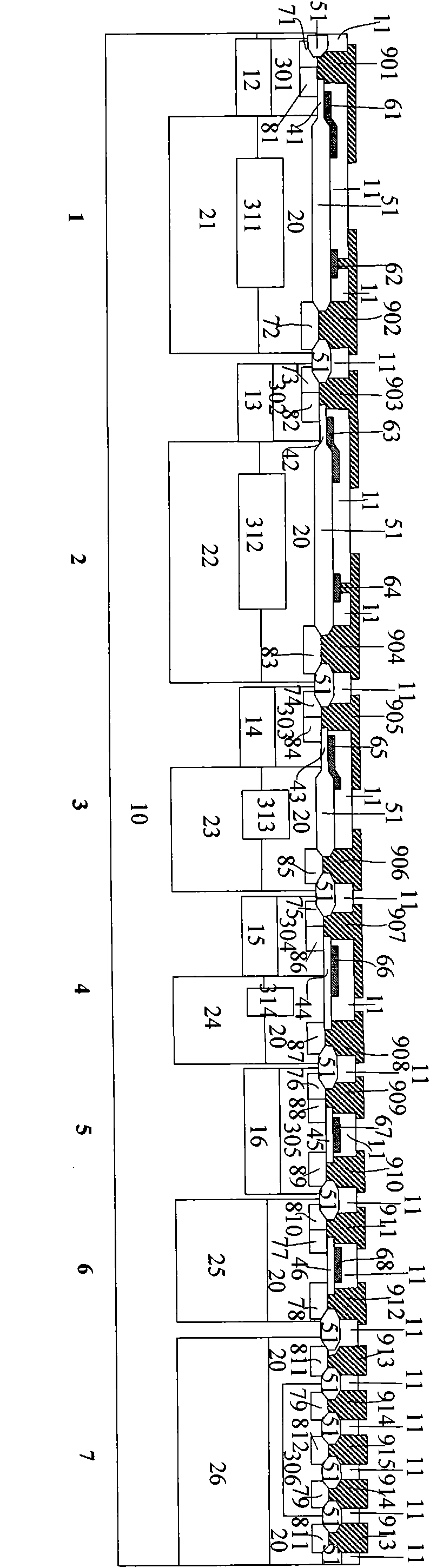
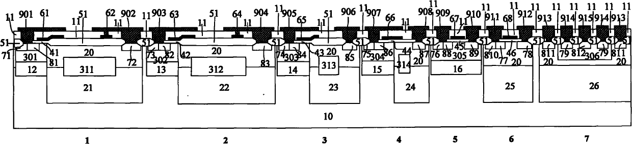
[0026] A BCD semiconductor device such as figure 1 As shown, including high-voltage nLIGBT device 1 integrated on the same chip, the first type of high-voltage nLDMOS device 2, the second type of high-voltage nLDMOS device 3, the third type of high-voltage nLDMOS device 4, low-voltage NMOS device 5, low-voltage PMOS device 6 and low-voltage NPN device7.

[0027] The high-voltage nLIGBT device 1 is directly made in the p-type substrate 10, and the p-type field drop layer 311 is located under the field oxide layer 51 and surrounded by the n-type drift region well 21 and the n-type epitaxial layer 20; p + The anode region 72 is under the anode metal 902 and surrounded by the n-type epitaxial layer 20; n + Cathode region 81 and p + The well contact region 71 is located side by side under the cathode metal 901 and is surrounded by the p-type body region 301; the p-type buried layer 12 is located between the p-type body region 301 and the p-type substrate 10; the polysilicon gate ...


PUM


Abstract

The invention discloses a BCD device and a manufacturing method thereof, which belong to the technical field of semiconductor power devices. In the invention, semiconductor devices such as a high-voltage nLIGBT, three high-voltage nLDMOSs, a low-voltage NMOS, a low-voltage PMOS, a low-voltage NPN and the like are synchronously integrated on the same chip, wherein the high-voltage nLIGBT, the high-voltage nLDMOSs and the low-voltage NPN are directly arranged on a single-crystal p-type substrate; the low-voltage NMOS is arranged in a p-type well; and the low-voltage PMOS is arranged in an n-type epitaxial layer. As p-type reduced-field layers are respectively arranged between the n-type epitaxial layer and an n-type shift region well, the n-type epitaxial layer on a p-type buried layer supplies an extra surface conducting channel to high-voltage devices, the conducting channel is increased, the specific on resistance of the high-voltage devices is reduced, and the manufacturing cost of the chip is further reduced. The nLIGBT device and the nLDMOS devices of the invention further have the characteristics of high input impedance, low output impedance and the like, and a high-voltage power integrated circuit formed by the nLIGBT device and the nLDMOS devices can be used in a plurality of products, such as consumer electronics, display drivers and the like.

Description

technical field [0001] The invention belongs to the technical field of semiconductor power devices. Background technique [0002] The development of high-voltage power integrated circuits is inseparable from high-voltage and low-voltage semiconductor devices. High-voltage power integrated circuits often use the high analog precision of Bipolar transistors, the high integration of CMOS, and the high power or voltage characteristics of DMOS (Double-diffused MOSFET) to integrate Bipolar analog circuits, CMOS logic circuits, CMOS analog circuits and DMOS high-voltage power devices. Monolithically integrated together (referred to as BCD device). Lateral high-voltage devices are widely used in high-voltage power integrated circuits because the drain, gate, and source are all on the chip surface, and are easy to integrate with low-voltage signal circuits through internal connections. However, due to the existence of Ron∝BV between the on-resistance Ron of the DMOS device and the ...

Claims


Application Information

Patent Timeline
Patent Type & Authority Applications(China)
IPC IPC(8): H01L27/06H01L29/06H01L29/10H01L21/8249
Inventor 乔明段双亮罗波蒋苓利傅达平张波
Owner UNIV OF ELECTRONICS SCI & TECH OF CHINA
Why Eureka
Try Eureka