Inverse epitaxial wafer preparation method

A technology of epitaxial wafers and epitaxial layers, applied in semiconductor/solid-state device manufacturing, gaseous chemical plating, coating, etc., can solve the problem of small expansion resistance surface at PN junction

Active Publication Date: 2011-11-30
HEBEI POSHING ELECTRONICS TECH
View PDF0 Cites 0 Cited by
  • Summary
  • Abstract
  • Description
  • Claims
  • Application Information

AI Technical Summary

Problems solved by technology

[0003] The technical problem to be solved by the present invention is to provide a method for preparing epitaxial wafers. In this method, the temperature in the furnace and the flow rate of hydrogen gas are increased when growing the intrinsic barrier layer to solve the current problem that the expansion resistance at the PN junction is smaller than that on the surface of the epitaxial layer.

Method used


Image

  • Inverse epitaxial wafer preparation method
  • Inverse epitaxial wafer preparation method
  • Inverse epitaxial wafer preparation method

Examples


Embodiment 1

[0019] 1) Pass hydrogen through the monolithic furnace, place the P-type substrate silicon wafer into the monolithic furnace with a manipulator at 800-950°C, raise the temperature to 1140°C, and the hydrogen flow rate is 20L / min;

[0020] 2) Baking to remove the oxide layer, the time is 1min, the hydrogen flow rate is 20L / min;

[0021] 3) Conduct chemical vapor phase polishing with hydrogen chloride for 1 minute, the flow rate of hydrogen chloride is 0.3L / min, and the flow rate of hydrogen gas is 20L / min;

[0022] 4) Raise the temperature of the single-chip furnace to 1170°C, and increase the hydrogen flow rate to 100L / min;

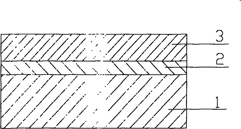
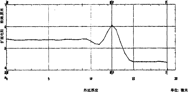
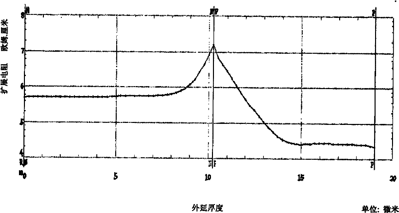
[0023] 5) The intrinsic barrier layer is grown by trichlorosilane, the trichlorosilane flow rate: 3L / min, and the growth time is 10 seconds; the intrinsic barrier layer produced is single crystal intrinsic silicon;

[0024] 6) Turn off the trichlorosilane, keep the temperature within the range of 1170°C, and expel the gas for 50 seconds at a hydrogen flo...

Embodiment 2

[0029] 1) Pass hydrogen through the single-chip furnace, place the P-type substrate silicon wafer into the single-chip furnace with a robot at 950°C, raise the temperature to 1150°C, and the hydrogen flow rate is 80L / min;

[0030] 2) Baking to remove the oxide layer, the time is 3min, the hydrogen flow rate is 80L / min;

[0031] 3) Conduct chemical vapor phase polishing with hydrogen chloride for 1 minute, hydrogen chloride flow rate 1L / min, hydrogen flow rate 80L / min;

[0032] 4) Raise the temperature of the single-chip furnace to 1210°C, and increase the hydrogen flow rate to 200L / min;

[0033] 5) The intrinsic barrier layer is grown by trichlorosilane, the trichlorosilane flow rate: 8L / min, and the growth time is 60 seconds; the intrinsic barrier layer produced is single crystal intrinsic silicon;

[0034] 6) Turn off the trichlorosilane, keep the temperature within the range of 1210°C, and catch the gas for 120 seconds at a hydrogen flow rate of 200L / min;

[0035] 7) Redu...

Embodiment 3

[0039] 1) Pass hydrogen through the single-chip furnace, place the P-type substrate silicon wafer into the single-chip furnace with a robot at 900°C, raise the temperature to 1145°C, and the hydrogen flow rate is 60L / min;

[0040] 2) Baking to remove the oxide layer, the time is 2min, the hydrogen flow rate is 60L / min;

[0041] 3) Perform chemical vapor phase polishing with hydrogen chloride for 1 minute, the flow rate of hydrogen chloride is 0.7L / min, and the flow rate of hydrogen gas is 60L / min;

[0042] 4) Raise the temperature of the single-chip furnace to 1200°C, and increase the hydrogen flow rate to 150L / min;

[0043] 5) The intrinsic barrier layer is grown by trichlorosilane, the flow rate of trichlorosilane is 6L / min, and the growth time is 40 seconds; the intrinsic barrier layer produced is single crystal intrinsic silicon;

[0044] 6) Turn off the trichlorosilane, keep the temperature within the range of 1200°C, and expel the gas for 80 seconds at a hydrogen flow r...


PUM


Abstract

The invention relates to a method for preparing an epitaxial wafer, in particular to a method for preparing an inverse epitaxial wafer for preparing an N-type epitaxial layer on a P-type substrate. This method breaks the traditional process of preparing epitaxial wafers with constant temperature and hydrogen flow rate, and increases the temperature in the monolithic furnace and the flow rate of hydrogen gas when preparing the intrinsic barrier layer, so that a large number of system impurities are eliminated. It is taken out of the reaction chamber to increase the cleanliness of the system and ensure the high resistivity of the intrinsic barrier layer. Even if the grown intrinsic barrier layer has higher purity, it has a stronger ability to prevent the expansion of substrate impurities.

Description

technical field [0001] The invention relates to a method for preparing an epitaxial wafer, in particular to a method for preparing an inverse epitaxial wafer for preparing an N-type epitaxial layer on a P-type substrate. Background technique [0002] The reverse epitaxial wafer refers to the epitaxial wafer in which the N-type epitaxial layer is prepared on the P-type substrate. At present, the preparation process used in production is: when the furnace temperature reaches 800-950°C, place the silicon wafer in the furnace with a manipulator, and pass through the hydrogen gas. ~1150℃, after baking, pass through hydrogen chloride for gas phase polishing; close hydrogen chloride, pass through trichlorosilane to produce intrinsic barrier layer; close trichlorosilane, use hydrogen to remove impurity gas in the furnace, and then pass through three Chlorosilane and PH 3 , grow the epitaxial layer, and finally lower the temperature to 800-950°C and take out the silicon wafer with ...

Claims


Application Information

Patent Timeline
Patent Type & Authority Patents(China)
IPC IPC(8): H01L21/205C23C16/44
Inventor 赵丽霞高国智
Owner HEBEI POSHING ELECTRONICS TECH
Why Eureka
Try Eureka