

Method for preparing selective emitter by one-time diffusion
An emitter and selective technology, applied in the direction of climate sustainability, final product manufacturing, sustainable manufacturing/processing, etc., can solve the problems of complex process, difficult control, high production cost, etc., and achieve simple process, easy control, low cost effect
- Summary
- Abstract
- Description
- Claims
- Application Information
AI Technical Summary
Problems solved by technology
Method used
Image

Examples
preparation example Construction
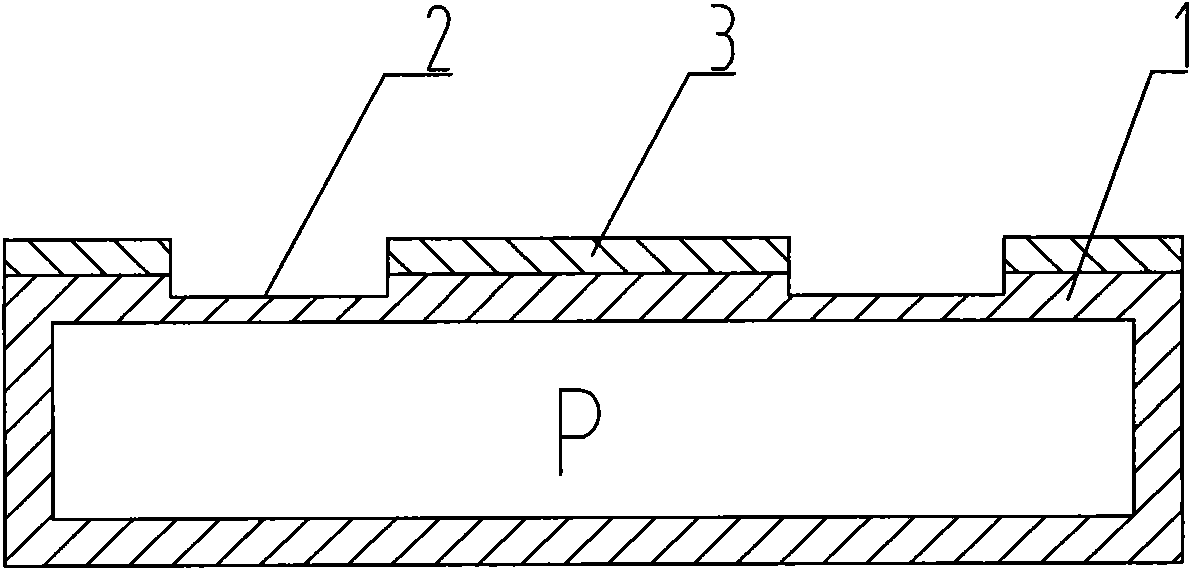
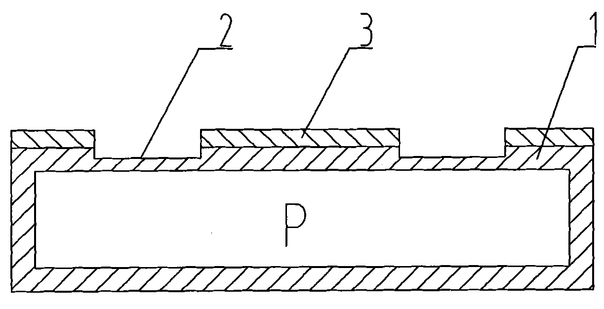
[0018] The preparation of the shallow diffusion junction here is to slowly etch the heavy diffusion area with an acid solution or an alkali solution, and the shallow diffusion area 2 is obtained by controlling the concentration ratio, time, and temperature of the acid solution or alkali solution. The acid solution here is HF acid and HNO 3 The mixed solution, in which the concentration of HF acid is 20-150g / l, HNO 3 The concentration is 20-350g / l; the alkali solution is KOH solution or NaOH solution, and the concentration of KOH solution or NaOH solution is 0.1wt%-5wt%; the corrosion time with acid solution or alkali solution is 1-30min, and the temperature is 5-90 ℃. In this way, by controlling the solution ratio, reaction temperature and time, the corrosion rate can be controlled at about 0.1um / min.
[0019] The structure of the selective emitter prepared by this method has no damage on the surface, the surface concentration of the shallow diffusion zone 2 is lower than th...
Embodiment 1
[0021] Select a P-type single-crystal silicon wafer with a crystal plane (100) and a doping concentration of 2.5Ωcm. The surface of the silicon wafer is textured by normal solar cell technology, and then re-diffused to obtain a sheet resistance of 25ohm / Sq. Plating an 80nm SiN film on the surface, and then printing a corrosive slurry on the non-electrode area, after washing off the etch, the concentration ratio is HNO 3 100g / l, 35g / l HF acid solution, the process temperature is 5°C, and the time is 5min. As the process progresses, the heavy diffusion region 1 not covered by the silicon nitride film 3 will be etched slowly. The total etching thickness is 0.6um, and then use 10% HF acid to wash away the SiN shielding film in the electrode area, and then perform other subsequent normal selective diffusion solar cell processes such as anti-reflection film coating, front and back electrode printing and sintering according to the process requirements .
PUM
| Property | Measurement | Unit |
|---|---|---|
| thickness | aaaaa | aaaaa |
Abstract
Description
Claims
Application Information