Two dimension electro-optical switch array device based on microfluidic technology

An electro-optical switch array and microfluidic technology, applied in the field of optical communication, can solve the problems of large power consumption, large size, slow corresponding speed, etc., and achieve the effects of easy fabrication, low cost and simple structure

Inactive Publication Date: 2010-08-11
NANJING UNIV OF POSTS & TELECOMM
View PDF1 Cites 12 Cited by
  • Summary
  • Abstract
  • Description
  • Claims
  • Application Information

AI Technical Summary

Problems solved by technology

On the one hand, the simultaneous installation of waveguides, heaters or lasers and containers on the substrate requires very precise and complex and cumbersome processing techniques, and the volume is not small; on the other hand, the integration level is not high, the corresponding speed is relatively slow, and the power consumption is low. Not small

Method used


Image

  • Two dimension electro-optical switch array device based on microfluidic technology
  • Two dimension electro-optical switch array device based on microfluidic technology
  • Two dimension electro-optical switch array device based on microfluidic technology

Examples


specific Embodiment 1

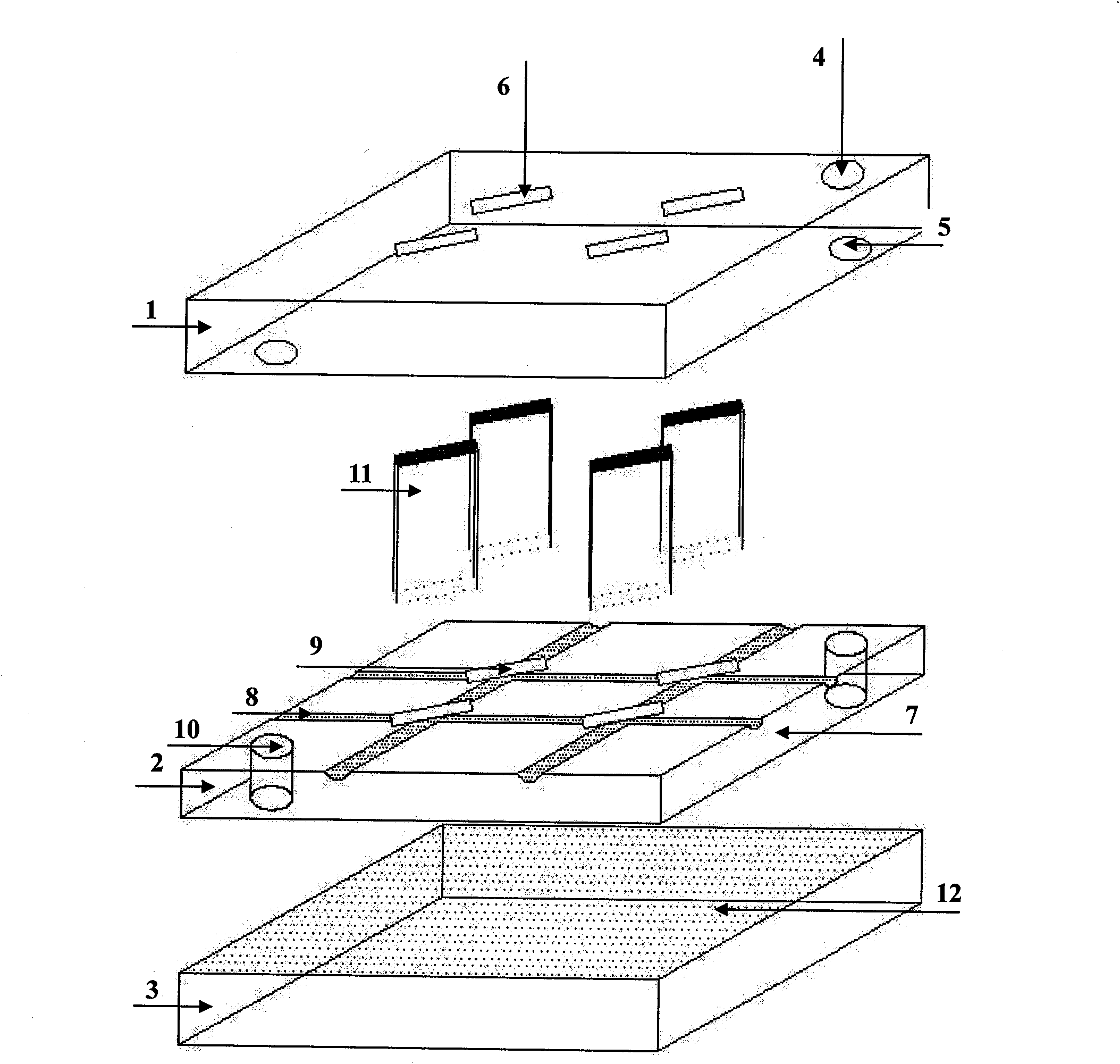
[0036] The waveguide layer is made of BK7 optical glass as the waveguide substrate. Because there are few internal impurities and defects, and the size of the internal defects is small compared with the light wavelength, the absorption loss and scattering loss are relatively low. The preparation method of the waveguide structure arranged in matrix form is through conventional coating, photolithography process and Ag + --Na + and K + --Na + ion exchange technology. At the node of the waveguide, a liquid chamber groove with the same size as the micro-container of the switch unit is made by ultrasonic method, and a gas-liquid connection hole is made at a convenient place on the substrate. The glass material with the same refractive index as the waveguide is selected to make the switch unit micro-container, and a transparent ITO conductive layer is sputtered on the inner side except the side facing the incident light. The insulating layer outside the conductive layer adopts th...

specific Embodiment 2

[0038] The waveguide layer uses monocrystalline silicon as the waveguide substrate, and micro-grooves are engraved on the waveguide position. A cylindrical lens is placed in each trench, and its central axis is on the same horizontal plane, and they are arranged in parallel or perpendicular to each other. The central axis extension lines of the four segments of cylindrical lenses around the optical switch unit intersect at a point on the surface of the optical switch unit. Silicone oil is used as the refractive index matching liquid of the device, which is also doped with some ether reagents until the refractive index is the same as that of the wall of the micro-container of the switch unit.


PUM


Abstract

The invention relates to a two dimension electro-optical switch array device based on a microfluidic technology, adopting a structure of an air storage layer plus a waveguide layer plus a fluid storage layer, wherein, the waveguide layer comprises a flat basement (7), a waveguide structure (8) which is arranged in a matrix form is arranged on the basement, a fluid cavity (9) is arranged at a waveguide cross node, the edge of the basement is provided with an air-fluid connecting channel (10),and an electronic control optical switch unit array (11) is arranged at the fluid cavity (9) at the waveguide cross node; the air storage layer is a sealing container (1) which stores the air, the edge of the container is provided with an air pressure adjusting control hole (4), an air-fluid connecting open hole (5) at the bottom part penetrates the waveguide layer and is communicated with the fluid storage layer, an electrode open hole (6) which is consistent with the waveguide cross node is arranged on the container, thereby being convenient to show an optical switch control unit electrode (18); the fluid storage layer is a container which is open ended at the upper end and stores the fluid, the fluid storage layer is sealed through combining the waveguide layer, the microcontainer inner surface tension is changed through an electro wetting effect to adjust the height of a liquid column, thereby realizing total reflection and total transmission of a light beam and further realizing the opening and closing actions of the light.

Description

technical field [0001] The invention relates to a novel two-dimensional electro-optic switch array structure and its working principle, belonging to the technical field of optical communication. Background technique [0002] The optical switch is the core device of optical switching, and it is also one of the main factors affecting the performance of the optical network. As a key device of the new-generation all-optical networking network, the optical switch is mainly used to realize functions such as routing selection, wavelength selection, optical cross-connection and self-healing protection on the optical level. In an all-optical network, optical add-drop multiplexing devices (OADM) and optical cross-connects (OXC) are indispensable network node devices, and optical switches and optical switch arrays are the core devices in these devices. With the continuous progress of understanding and research on device materials, device working principles, and processing technology, ...

Claims


Application Information

Patent Timeline
Patent Type & Authority Applications(China)
IPC IPC(8): G02B6/35G02B26/02
Inventor 陈陶梁忠诚徐宁江博
Owner NANJING UNIV OF POSTS & TELECOMM
Why Eureka
Try Eureka