Method for preparing nanoparticles of inorganic material and device for applying same

A nanoparticle and inorganic material technology, applied in the fields of nanostructure manufacturing, nanotechnology, nanotechnology, etc., can solve problems such as poor efficiency, time-consuming, and inability to manufacture nanoparticles in a large area, achieving good manufacturing efficiency and reducing manufacturing costs. cost effect

Inactive Publication Date: 2010-08-18
林宽锯
View PDF2 Cites 2 Cited by
  • Summary
  • Abstract
  • Description
  • Claims
  • Application Information

AI Technical Summary

Problems solved by technology

[0006] (i) High temperature annealing (High temperature annealing): There must be a period of heating and cooling time during the process, resulting in a long time-consuming and poor efficiency, and due to the long time required for heating and cooling, the formed nano The morphology of the particle surface is not easy to be uniform, and it is easy to aggregate into particles with larger particle size
[0007] (ii) Electron beam local bombardment (e-beam irradiation): requires the use of expensive instruments and equipment - electron guns. In addition, the electron gun has a limited range of action each time, resulting in a limited surface for one treatment, and it is impossible to manufacture nano-particles on the substrate in a large area. Particles, also have the absence of less efficient manufacturing
[0008] (iii) Heavy ion beam local bombardment (heavy ion irradiation): Like electron beam bombardment, it requires the use of expensive instruments and equipment, and can only be processed locally at a time and cannot produce nanoparticles in a large area. It also has the disadvantage of poor manufacturing efficiency. , the current application level is still limited to academic research
[0009] (iv) Pulsed laser irradiation: It can only process a small area at a time. Although it can achieve the effect of processing a larger area by continuously moving back and forth, it takes a relatively long time and the area that can be processed is still limited. This method also has the disadvantage of poor manufacturing efficiency
[0010] (v) Nanolithography: Although this method can produce a large number of nanoparticle arrays on the substrate, the steps are very cumbersome, time-consuming and need to be washed with organic solvents during the process, and the manufacturing efficiency is poor and less environmentally friendly missing

Method used


Image

  • Method for preparing nanoparticles of inorganic material and device for applying same
  • Method for preparing nanoparticles of inorganic material and device for applying same
  • Method for preparing nanoparticles of inorganic material and device for applying same

Examples


Embodiment 1

[0053]

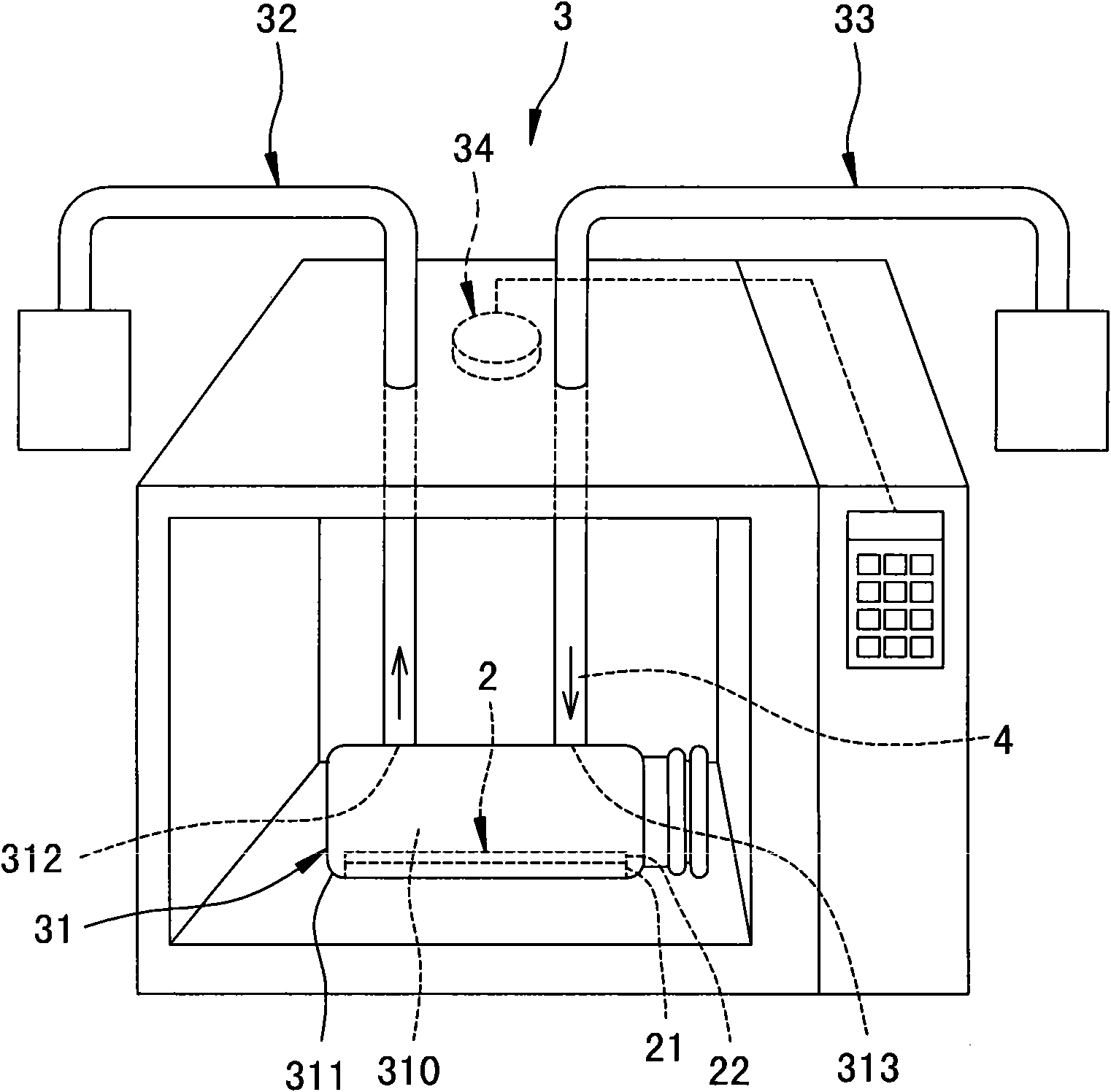
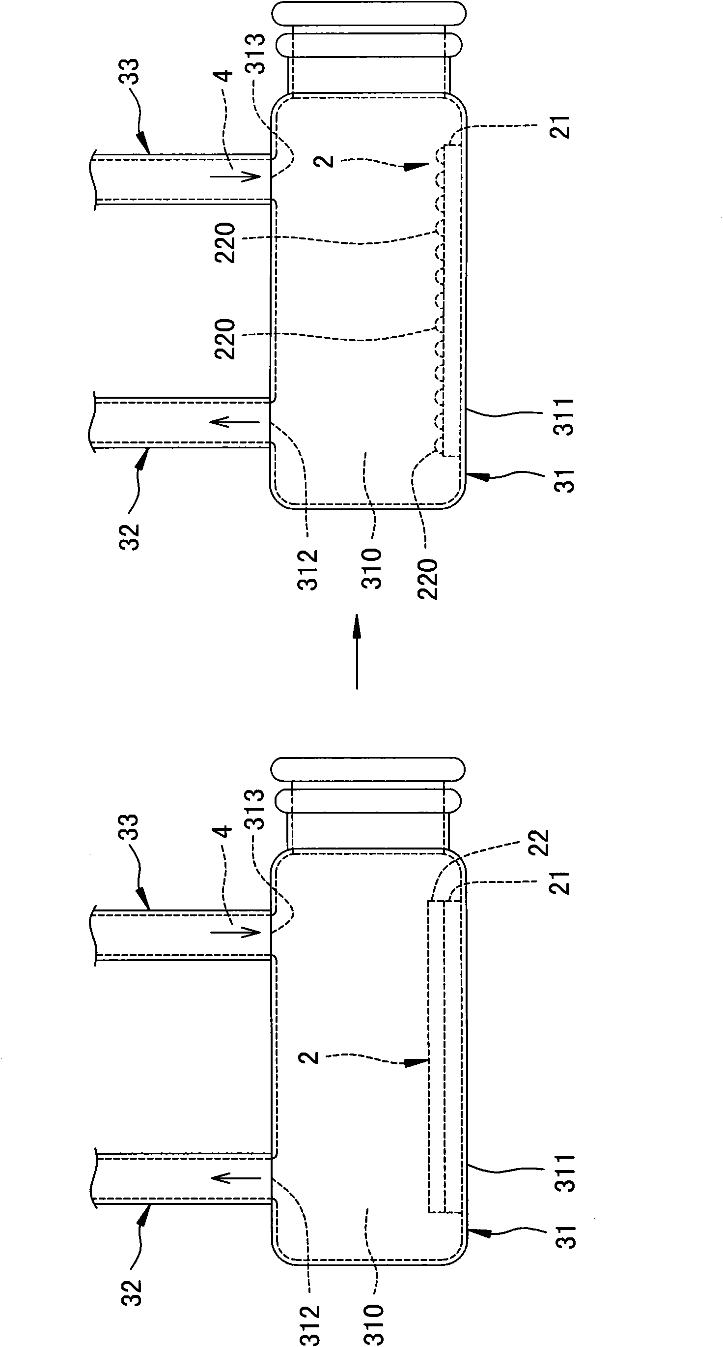
[0054] (1) Prepare 8 pieces of composite components: cut into 1 cm × 1 cm base material, 8 pieces in total, put the base material into acetone, ethanol, and deionized water respectively, and vibrate for 5 minutes under ultrasonic waves, with Remove some dust contamination from the surface of the substrate. Then use nitrogen to dry the surface of all substrates, and then soak the substrates in a piranha solution (piranha solution, H 2 SO 4 with H 2 o 2 Mixed according to the ratio of 3:1, and the temperature of 80 ℃ mixed liquid) for 30 minutes to remove some organic residues on the surface of the substrate, and then rinse with a large amount of deionized water, and then nitrogen gas Substrate blow dry completely.

[0055] Put the 8 pieces of substrates that have been cleaned through the aforementioned procedures into a sputtercoater, and use a film thickness controller to control the thickness of the inorganic material layer sputtered on the substrate to the req...

Embodiment 2

[0059]

[0060]With the preparation method of , prepare 5 clean substrate sheets, and form inorganic material layers with a thickness of 1nm, 2nm, 3nm, 4nm, and 5nm on the substrate sheets respectively, and the corresponding microwave The action time of the energy is 3 seconds, 6 seconds, 9 seconds, 12 seconds, and 15 seconds respectively. The device used and the setting parameters are the same as in , except that the material of the inorganic material layer is changed to silver , after microwave plasma treatment, the composite components with different thicknesses of inorganic material layers are processed by microwave plasma and the nanoparticles formed on the substrate are changed from thin to thick according to the thickness of the original inorganic material layer, respectively Marked as Specimen (II 1 ), (II 2 ), (II 3 ), (II 4 ), (II 5 ), the obtained result is as Image 6 and Figure 7 As shown, it shows that the particle size of the nanoparticles still increas...

Embodiment 3

[0061]

[0062] Similar to the method of , prepare 5 clean substrate sheets, and form inorganic material layers with a thickness of 1nm, 2nm, 3nm, 4nm, and 5nm on the substrate sheets, and the corresponding The action time of microwave energy is respectively 15 seconds, 18 seconds, 21 seconds, 24 seconds, and 27 seconds. The device used and the setting parameters are the same as , except that the material of the inorganic material layer is changed to copper, and The pressure of the chamber is controlled at 1.0 torr, and oxygen is fed into the chamber to prepare microwave plasma nanoparticles in an oxygen environment. After microwave plasma treatment, the composite components with different thicknesses of inorganic material layers The nanoparticles prepared after microwave plasma treatment and formed on the substrate are marked as samples (III) according to the thickness of the inorganic material layer from thin to thick. 1 ), (III 2 ), (III 3 ), (III 4 ), (III 5 ), the o...


PUM

PropertyMeasurementUnit
thicknessaaaaaaaaaa
particle diameteraaaaaaaaaa
thicknessaaaaaaaaaa

Abstract

The invention discloses a method for preparing nanoparticles of an inorganic material and a device for applying the same. The preparation method comprises the following steps: providing a composite component, wherein the composite component is provided with a base material and at least one inorganic material layer which is formed on the base material and has a predetermined thickness; putting the composite component in a cavity; vacuumizing the cavity; providing a gas; and providing a microwave energy continuously for the cavity in a predetermined time period, so that the gas forms a microwave plasma, and applying the microwave plasma to the inorganic material layer of the composite component, so that the inorganic material layer is melted to form nanoparticles having a plurality of phase intervals and a predetermined particle size. Therefore, a great amount of nanoparticles having the predetermined particle size can be prepared in a short time by using a simpler device and method according to the invention; and the invention has the advantages of low preparation cost and excellent preparation efficiency.

Description

【Technical field】 [0001] The present invention relates to a method and a manufacturing device of nanoparticles, in particular to a method of manufacturing nanoparticles of inorganic materials which is convenient for mass production and has better manufacturing efficiency and a device using the method. 【Background technique】 [0002] Nanotechnology is one of the focuses of current technological development. Since the application of nanomaterials can make products have the characteristics of lightness, lightness, energy saving, high capacity density, high precision, high performance and low pollution, it will bring the impetus to the upgrading of traditional industries and the sustainable development and sustainable development of high-tech industries. Make nanomaterials the cornerstone of the development of nanotechnology. Therefore, researchers in the fields of materials, physics, chemistry, chemical industry and biology have invested in the research and development of nanot...

Claims


Application Information

Patent Timeline
Patent Type & Authority Applications(China)
IPC IPC(8): B82B3/00
Inventor 林宽锯许纯渊
Owner 林宽锯
Why Eureka
Try Eureka