

Preparation method for hydrogenated crystalline state nanometer carborundum films under low temperature
A technology of silicon carbide and nanocrystals, applied in the direction of gaseous chemical plating, metal material coating process, coating, etc., can solve problems affecting film properties, defects, high stress and lattice, and achieve the effect of avoiding damage
- Summary
- Abstract
- Description
- Claims
- Application Information
AI Technical Summary
Problems solved by technology
Method used
Image

Examples
Embodiment 1
[0025] The method for preparing a hydrogenated nanocrystalline silicon carbide film at a low temperature according to the first embodiment of the present invention comprises the following steps:
[0026] A. Take a single crystal silicon wafer substrate, clean it in an ultrasonic cleaner for 3 minutes with a mixture of acetone and methanol, then dry it, and then use a volume ratio NH 4 OH:H 2 o 2 :H 2 O=1:2:5 mixed solution soaked for 5 minutes, took out and rinsed with deionized water, and then put in the volume ratio HF:H 2 Soak in the mixed solution of O=1:10 for 1 minute, take it out and rinse it with deionized water, dry it and place it on the substrate stage of the helicon wave plasma enhanced chemical vapor deposition device;
[0027] B. Use the vacuum pumping system of the helicon wave plasma enhanced chemical vapor deposition device to evacuate the reaction chamber until the pressure in the reaction chamber is lower than 1×10 -4 Pa;
[0028] C. Pass hydrogen gas w...
Embodiment 2
[0032]The method for preparing a hydrogenated nanocrystalline silicon carbide film at a low temperature in the second embodiment of the present invention has the same steps as in the embodiment 1, except that the substrate stage is heated to 300° C. in step 1-D.
Embodiment 3
[0034] The method for preparing a hydrogenated nanocrystalline silicon carbide film at a low temperature in the third embodiment of the present invention has the same steps as in the embodiment 1, except that the substrate stage is heated to 400° C. in step 1-D.
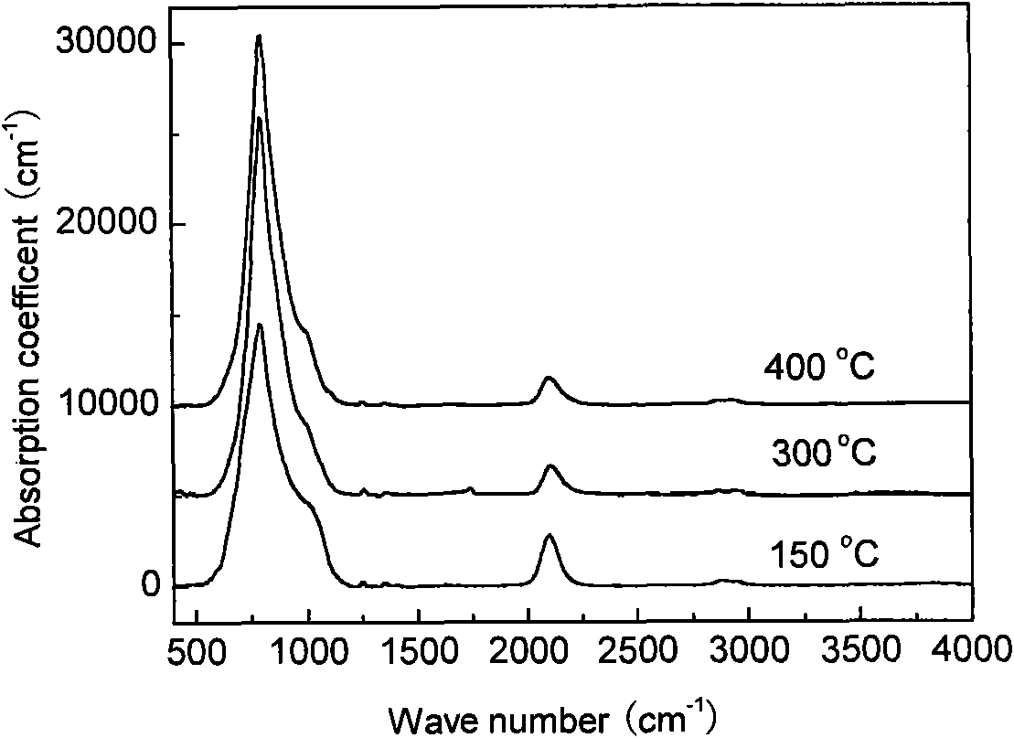
[0035] Embodiment 1-3 has adopted different substrate temperature, figure 1 The FTIR spectra of the hydrogenated nanocrystalline silicon carbide films obtained in Examples 1-3 are given, from which it can be seen that the absorption peaks associated with the Si-C stretching mode are respectively located at 793-798cm -1 Nearby, using the deconvolution method, for the three films at 500-1200cm -1 The absorption bands within the range are deconvoluted, and it is found that they all need Lorentzian peaks to fit the spectral lines, and the crystallinity increases significantly with the increase of the substrate temperature. The results show that the deposition of hydrogenated nanocrystalline silicon carbide films can be ...
PUM
 Abstract
Description
Claims
Application Information