LED with two-dimensional photonic crystals

A two-dimensional photonic crystal and light-emitting diode technology, which is applied to semiconductor devices, electrical components, circuits, etc., can solve the problems of low light-emitting efficiency of light-emitting diodes, increased non-radiative recombination, and damage to semiconductor active layers, and achieves high production costs. , Increase the brightness of the light output, improve the effect of the difference of the refraction law

Inactive Publication Date: 2010-08-25
HARBIN INST OF TECH
View PDF6 Cites 18 Cited by
  • Summary
  • Abstract
  • Description
  • Claims
  • Application Information

AI Technical Summary

Problems solved by technology

[0005] The purpose of the present invention is to solve the problems of low light extraction efficiency of existing light-emitting diodes and damage to the semiconductor active layer by traditional etching, photolithography or embossing techniques, resulting in increased non-radiative recombination. Two-dimensional photonic crystals for light-emitting diodes

Method used


Image

  • LED with two-dimensional photonic crystals
  • LED with two-dimensional photonic crystals
  • LED with two-dimensional photonic crystals

Examples


specific Embodiment approach 1

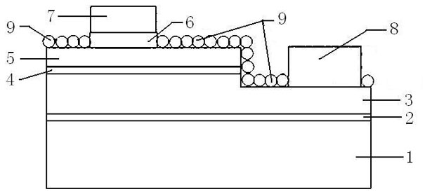
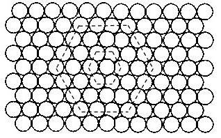
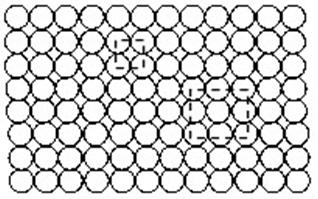
[0013] Specific Embodiment 1: This embodiment has a light-emitting diode with two-dimensional photonic crystals, including a substrate 1, a buffer layer 2, an N-type doped semiconductor layer 3, an active layer 4, a P-type doped semiconductor layer 5, and a current diffusion layer. 6. The P-type electrode 7 and the N-type electrode 8, the P-type electrode 7 is connected to the P-type doped semiconductor layer 5 through the current diffusion layer 6, and the N-type electrode 8 is directly connected to the N-type doped semiconductor layer 3, wherein The interface between the N-type doped semiconductor layer 3 and the air, and the interface between the P-type doped semiconductor layer 5 and the air are covered with a two-dimensional photonic crystal layer 9, and the two-dimensional photonic crystal layer 9 is a single-layer microsphere orderly arrangement structure , the particle size of the microspheres is 0.05 μm to 5 μm.

[0014] A schematic cross-sectional view of a light-emi...

specific Embodiment approach 2

[0016] Embodiment 2: This embodiment is different from Embodiment 1 in that the microspheres in the two-dimensional photonic crystal layer 9 are silicon dioxide microspheres, polystyrene microspheres or polymethyl methacrylate microspheres. Other parameters are the same as in the first embodiment.

specific Embodiment approach 3

[0017] Embodiment 3: The difference between this embodiment and Embodiment 1 is that the microspheres in the two-dimensional photonic crystal layer 9 are silicon dioxide microspheres, polystyrene microspheres or polymethylmethacrylate coated with metal on the outer layer. Ester microspheres where the metal is Ag, Pt, Au, Cu or Al. Other parameters are the same as in the first embodiment.


PUM


Abstract

The invention relates to a low cost LED with two-dimensional photonic crystals, and aims to solve the problem that the light-emitting efficiency is low and high production cost, and the problem that non-radiative recombination increases because a semiconductor active layer is damaged by adopting the conventional etching, photo-etching or imprinting technique in the conventional LED. The LED comprises a substrate, a buffer layer, an N-type doped semiconductor layer, an active layer, a P-type doped semiconductor layer, a current diffusing layer, a P-type electrode and an N-type electrode, wherein two-dimensional photonic crystal layers are covered on the interface between the N-type doped semiconductor layer and the air and the interface between the P-type doped semiconductor layer and the air; and the two-dimensional photonic crystal layer adopts a single-layer micro-sphere ordered arrangement structure, and the grain size of the micro-spheres is 50nm to 5 mu m. In the LED, by using the two-dimensional photonic crystal layer, a refraction index difference between the semiconductor and the outside is improved; and by utilizing the weak photonic crystal effect, a light-emitting efficiency is improved by 10 to 20 percent compared with that of the conventional LED. The LED of the invention is suitable for large-area and industrialized production.

Description

technical field [0001] The invention relates to a light-emitting diode with a photonic crystal. Background technique [0002] Light-emitting diodes are green, energy-saving, safe, durable, and long-lived semiconductor lighting devices. They gradually replace incandescent lamps and light bulbs as mainstream lighting products. Applications are increasing day by day. [0003] The internal quantum efficiency and external quantum efficiency of light-emitting diodes determine the light extraction efficiency and device brightness of light-emitting diodes. The theoretical value of the internal efficiency of light-emitting diodes can reach 100%. At present, the internal quantum efficiency of GaN light-emitting diodes is basically around 90%. Due to the bottleneck of semiconductor epitaxy technology, it is difficult to improve the internal quantum efficiency, and there is also room for improvement. limited. However, the external quantum efficiency of traditional light-emitting diod...

Claims


Application Information

Patent Timeline
Patent Type & Authority Applications(China)
IPC IPC(8): H01L33/02
Inventor 李垚詹耀辉赵九蓬丁艳波葛邓腾
Owner HARBIN INST OF TECH
Why Eureka
Try Eureka