Semiconductor memory unit, driving method thereof and semiconductor memory

A memory unit and semiconductor technology, applied in the field of semiconductors, can solve problems such as difficult to control, affect the yield of semiconductor memory, and not disclose single-chip systems, etc., and achieve the effect of device shrinkage

Inactive Publication Date: 2012-08-22
SEMICON MFG INT (SHANGHAI) CORP +1
View PDF0 Cites 0 Cited by
  • Summary
  • Abstract
  • Description
  • Claims
  • Application Information

AI Technical Summary

Problems solved by technology

[0006] However, in the above technical scheme, hafnium oxide (HfO 2 ) nanocrystal technology is still immature and difficult to control, which will affect the yield of semiconductor memory. At the same time, the research does not disclose how to use this structure to form a single-chip system.

Method used


Image

  • Semiconductor memory unit, driving method thereof and semiconductor memory
  • Semiconductor memory unit, driving method thereof and semiconductor memory
  • Semiconductor memory unit, driving method thereof and semiconductor memory

Examples


Embodiment Construction

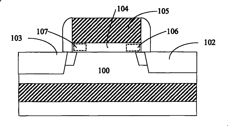
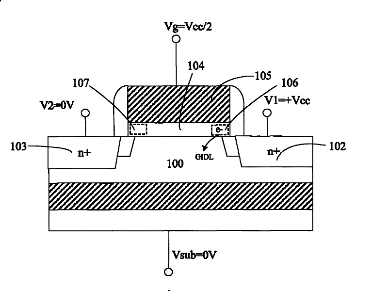
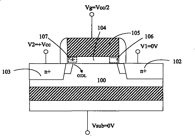
[0046] The present invention utilizes the existing SOI MOS transistor structure to form the first charge storage region and / or the second charge storage region in the gate dielectric layer through electric field force to form the required semiconductor memory unit without additional formation of the prior art The process of the memory unit is compatible with the existing logic circuit process, which improves the performance of the integrated circuit and reduces power consumption. At the same time, by using SOI as the semiconductor substrate, the leakage current of the semiconductor memory fabricated on it can be further reduced. Reduce power consumption, which is conducive to further shrinking of devices;

[0047] The electric field force of the present invention is formed by connecting different voltages on the first diffusion region, the second diffusion region, the gate electrode and the silicon substrate (equivalent to the body), between the gate electrode and the first dif...


PUM


Abstract

The invention relates to a semiconductor memory unit, a driving method thereof and a semiconductor memory, wherein the semiconductor memory unit comprises silicon on an insulator, a first diffusion region, a second diffusion region, a grid dielectric layer, a grid electrode, a first electric charge storage region and / or a second electric charge storage region, wherein the first diffusion region and the second diffusion region are positioned in top-layer silicon and mutually separated, and the conduction types of the first diffusion region and the second diffusion region are the same; the griddielectric layer and the grid electrode are sequentially positioned on the top-layer silicon above a channel region; and the first electric charge storage region and / or the second electric charge storage region are / is respectively positioned in the grid dielectric layer and close to the part between the channel region and the first diffusion region and in the grid dielectric layer and close to the part between the channel region and the second diffusion region, and the first electric charge storage region and / or the second electric charge storage region are / is formed through electric field force. In the invention, the first electric charge storage region and / or the second electric charge storage region are / is formed in the grid dielectric layer through the electric field force to form thememory unit, and the memory unit is compatible with a traditional logic circuit forming process, thereby improving the performance of an integrated circuit and reducing the power consumption.

Description

technical field [0001] The invention relates to the technical field of semiconductors, in particular to a semiconductor memory unit, a method for driving the semiconductor memory unit and a semiconductor memory. Background technique [0002] As CMOS continued to be highly integrated and high-performance, scale-down occurred, and very large-scale integration (VLSI) emerged. It is well known that scaling of existing CMOS technologies faces a trade-off between speed and power constraints at the 65nm node and below. Fortunately, mobility-enhancing stress engineering and new gate-stack materials (high-k and metal gates) can extend CMOS scaling below the 32nm node, where process complexity becomes more complex. Simultaneously, scaling down of DRAM and flash memory has resulted in continued shrinking of memory cell capacitance, select transistors, and charge storage layers. Unfortunately, the scaling down of CMOS logic and memory has made it more difficult to integrate them toget...

Claims


Application Information

Patent Timeline
Patent Type & Authority Patents(China)
IPC IPC(8): H01L27/12H01L29/792H01L29/06G11C16/10G11C16/14G11C16/26
Inventor 季明华肖德元
Owner SEMICON MFG INT (SHANGHAI) CORP
Why Eureka
Try Eureka