Method for preparing high-quality ZnO monocrystal film on sapphire substrate

A sapphire substrate and single crystal thin film technology, which is applied in semiconductor/solid-state device manufacturing, electrical components, circuits, etc., can solve problems such as small viscosity coefficient, short migration length, easy island growth, etc.

Inactive Publication Date: 2010-09-15
INST OF PHYSICS - CHINESE ACAD OF SCI
View PDF3 Cites 6 Cited by
  • Summary
  • Abstract
  • Description
  • Claims
  • Application Information

AI Technical Summary

Problems solved by technology

[0004] 2. Due to ZnO(0001) and α-Al 2 o 3 There is a lattice mismatch of 18.3% between (0001), how to fully release the huge lattice mismatch strain and control the nucleation and growth at the interface to prepare high-quality ZnO thin films is still a big challenge.
However, due to the great difference between oxides and nitrides in many aspects, compared with GaN, the preparation of ZnO thin films has a large saturated vapor pressure and low viscosity coefficient of Zn, which leads to short migration length and easy island growth. and other shortcomings, it is difficult to fully release the mismatch strain

Method used


Image

  • Method for preparing high-quality ZnO monocrystal film on sapphire substrate
  • Method for preparing high-quality ZnO monocrystal film on sapphire substrate
  • Method for preparing high-quality ZnO monocrystal film on sapphire substrate

Examples


Embodiment 1

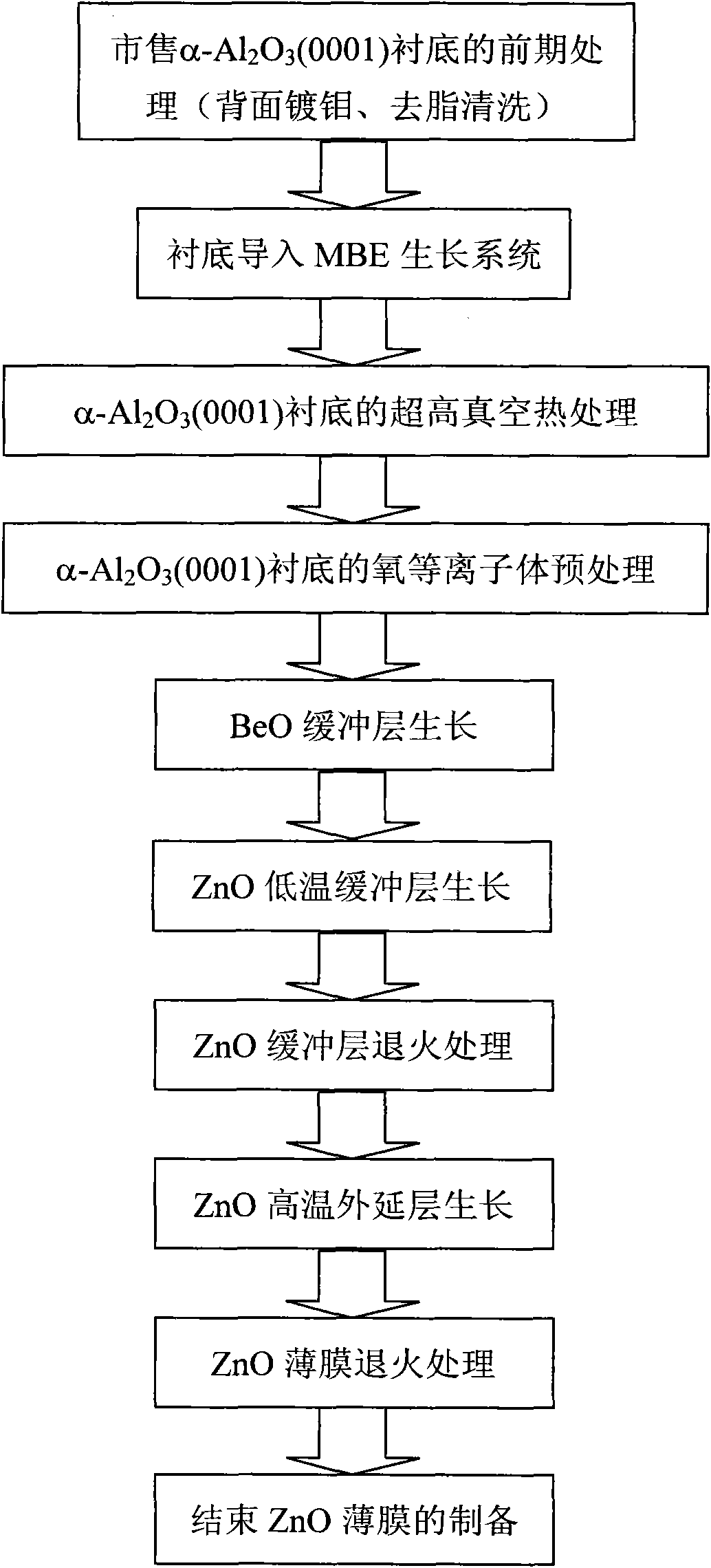
[0039] Such as figure 1 Shown process flow diagram of the present invention, the concrete steps of preparing high-quality ZnO single crystal thin film on sapphire (0001) substrate are as follows:

[0040] 1. Use known methods to carry out molybdenum plating on the back of the commercially available sapphire (0001) substrate, and perform chemical degreasing and cleaning, and then import the substrate into the MBE system;

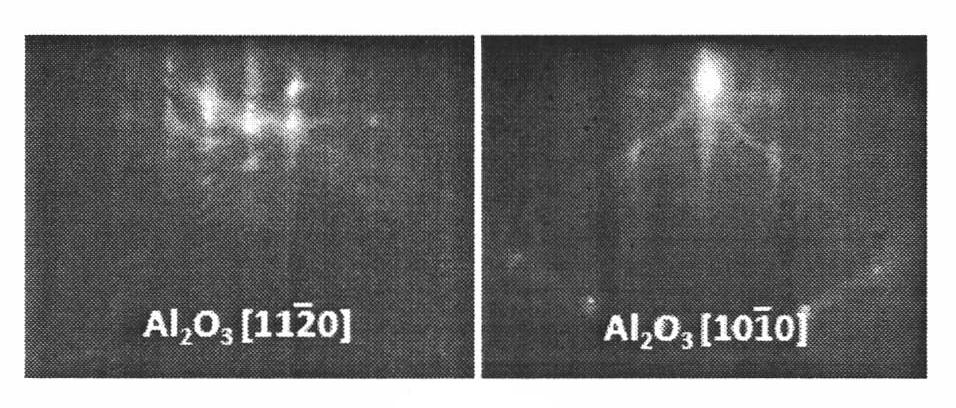
[0041] 2. First in ultra-high vacuum (not less than 1×10 -8 mbar) conditions, the substrate is heated to 700°C for 30 minutes of heat treatment, and then the substrate surface is treated with active oxygen plasma for 30 minutes at 100°C, the radio frequency power is 300W, and the oxygen flow rate is 2.0sccm;

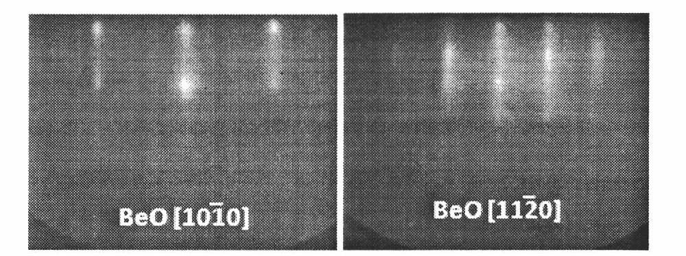
[0042] 3. The epitaxial growth of the BeO buffer layer is carried out at a substrate temperature of 500°C, and the equivalent vapor pressure of the Be beam is 5x10 -4 Around Pa, a thin layer of BeO with a thickness of about 2nm is obtained;

[0043] ...

Embodiment 2

[0050] Such as figure 1 Shown process flow diagram of the present invention, the concrete steps of preparing high-quality ZnO single crystal thin film on sapphire (0001) substrate are as follows:

[0051] 1. Use known methods to carry out molybdenum plating on the back of the commercially available sapphire (0001) substrate, and perform chemical degreasing and cleaning, and then import the substrate into the MBE system;

[0052] 2. First, in ultra-high vacuum (not less than 1×10 -8 mbar) conditions, the substrate is heated to 800°C for 20 minutes of heat treatment, and then the surface of the substrate is treated with active oxygen plasma at 300°C for 20 minutes, the radio frequency power is 300W, and the oxygen flow rate is 2.0sccm;

[0053] 3. The epitaxial growth of the BeO buffer layer is carried out under the condition of the substrate temperature of 1000°C, and the equivalent vapor pressure of the Be beam is 5x10 -4 Around Pa, a thin layer of BeO with a thickness of ab...

Embodiment 3

[0060] Such as figure 1 Shown process flow diagram of the present invention, the concrete steps of preparing high-quality ZnO single crystal thin film on sapphire (0001) substrate are as follows:

[0061] 1. Use known methods to carry out molybdenum plating on the back of the commercially available sapphire (0001) substrate, and perform chemical degreasing and cleaning, and then import the substrate into the MBE system;

[0062] 2. First in ultra-high vacuum (not less than 1×10 -8 mbar), the substrate is heated to 900°C for 10 minutes of heat treatment, and then the surface of the substrate is treated with active oxygen plasma at 500°C for 10 minutes, the radio frequency power is 300W, and the oxygen flow rate is 2.0sccm;

[0063] 3. The epitaxial growth of the BeO buffer layer is carried out at a substrate temperature of 1500°C, and the equivalent vapor pressure of the Be beam is 5x10 -4 pa, obtain a thin layer of BeO with a thickness of about 30nm;

[0064] 4. Deposit a Z...


PUM

PropertyMeasurementUnit
thicknessaaaaaaaaaa
thicknessaaaaaaaaaa
thicknessaaaaaaaaaa

Abstract

The invention discloses a method for preparing a high-quality ZnO monocrystal film on a sapphire substrate, which is the method for preparing the high-quality ZnO monocrystal film on the sapphire substrate by a surface, interface and buffer layer combined growth method and comprises the following concrete steps of: carrying out ultrahigh vacuum heat processing combined with oxygen plasma preprocessing on the surface of the sapphire (0001) substrate; then depositing a BeO buffer layer to supply an ideal template for the epitaxial growth of ZnO, and then preparing the high-quality ZnO film by a publicly known two-step growth method. The ZnO monocrystal film prepared according to the method has very good crystallization performance and is applicable for the manufacture of high-performance photoelectronic devices such as an ultraviolet detector and the like.

Description

technical field [0001] The invention relates to the field of ZnO single crystal film preparation, in particular to a method for preparing high-quality ZnO single crystal film on a sapphire substrate. Background technique [0002] As the core basic material of the third-generation semiconductor, ZnO has very superior photoelectric properties, its room temperature bandgap is 3.37eV, and the free exciton binding energy is 60meV. An important wide-bandgap semiconductor material has a very broad application prospect in the preparation of high-performance short-wavelength optoelectronic devices. In order to realize its device application, the preparation of high-quality ZnO-based epitaxial film is an important basis. Although the ZnO single crystal substrate has been commercialized, its price is still very expensive at present. Therefore, the homoepitaxial growth technology of ZnO single crystal thin film cannot realize its industrial application at present, so the heterogeneous ...

Claims


Application Information

Patent Timeline
Patent Type & Authority Applications(China)
IPC IPC(8): H01L21/205
Inventor 梅增霞梁会力梁爽刘章龙李俊强侯尧楠刘尧平崔秀芝张生利杜小龙
Owner INST OF PHYSICS - CHINESE ACAD OF SCI
Why Eureka
Try Eureka