
Silicon carbide epitaxial wafer and process for production thereof, silicon carbide bulk substrate for epitaxial growth purposes and process for production thereof, and heat treatment apparatus

一种热处理装置、制造方法的技术,应用在晶体生长、单晶生长、单晶生长等方向,能够解决自由度限制、晶片面均匀性降低、器件特性恶化等问题,达到良好生产性、平坦性好、缩短制作时间的效果

Active Publication Date: 2013-01-02
MITSUBISHI ELECTRIC CORP
View PDF6 Cites 10 Cited by
  • Summary
  • Abstract
  • Description
  • Claims
  • Application Information

AI Technical Summary

Problems solved by technology

That is, the conductivity decreases with the degree of mobility, and the device characteristics deteriorate
Therefore, in the presence of step bunching, there is a problem that the in-plane uniformity of the conductivity decreases.
Therefore, in the presence of step bunching, in devices such as MOS devices that induce carriers near the surface of the epitaxial growth layer, the degree of freedom in the design stage and manufacturing stage of the specific structure is significantly restricted.

Method used


Image

  • Silicon carbide epitaxial wafer and process for production thereof, silicon carbide bulk substrate for epitaxial growth purposes and process for production thereof, and heat treatment apparatus
  • Silicon carbide epitaxial wafer and process for production thereof, silicon carbide bulk substrate for epitaxial growth purposes and process for production thereof, and heat treatment apparatus
  • Silicon carbide epitaxial wafer and process for production thereof, silicon carbide bulk substrate for epitaxial growth purposes and process for production thereof, and heat treatment apparatus

Examples


Embodiment approach 1

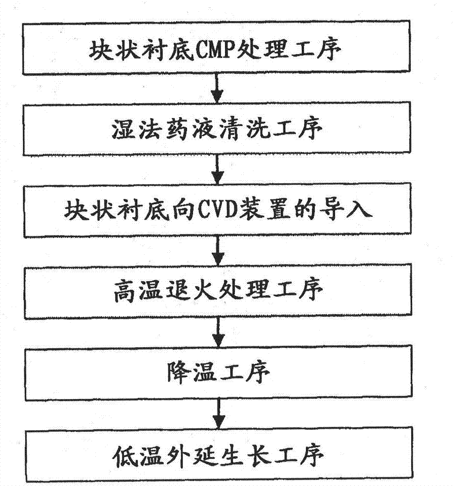
[0070] figure 1 It is a process flowchart showing the manufacturing procedure of the SiC epitaxial wafer in Embodiment 1 of the present invention.

[0071] The SiC bulk substrate used in the present invention is a 4H-SiC type substrate, which is inclined at an angle smaller than about 5 degrees from to the direction. In addition, the direction of inclination is not strictly limited to the direction, and a substrate of a specification that inclines in other directions may be used.

[0072] First, the SiC bulk substrate is planarized (CPM treatment) by preliminarily mechanical polishing and chemical mechanical polishing using an acidic or alkaline chemical solution. The planarized SiC bulk substrate is cleaned with ultrasonic waves using acetone or the like to remove organic substances adhering to the surface. Next, sulfuric acid and hydrogen peroxide aqueous solutions were mixed at a volume ratio of 5:1, and the SiC bulk substrate was immersed in the mixed solution heated ...

Embodiment approach 2

[0103] In the first embodiment, the annealing temperature dependence of the surface state of the SiC bulk substrate was described in detail. Generally, in the annealing treatment, the annealing temperature T1 and the treatment time t are important factors. That is, the above two parameters must be considered simultaneously for the effect of the annealing treatment on the wafer. In general, it can be said that the higher the annealing temperature T1 and the longer the treatment, the greater the degree of heat treatment. That is, the product of the annealing temperature T1 and the annealing time t, T1×t, directly indicates the degree of heat treatment. In addition, as described above, the experimental results in Table 1 also teach that the optimum treatment time t changes according to the annealing temperature T1. That is, as a principle, the higher the annealing temperature T1 and the shorter the processing time t, the defect density tends to decrease.

[0104] The treatment...

Embodiment approach 3

[0109] In Embodiment 1 and Embodiment 2, the annealing temperature dependence of the surface state of the epitaxial wafer, and the dependence of the defect density on the annealing temperature T1 and the annealing time t are described in detail. That is, a method for obtaining a high-quality epitaxial growth layer having a low defect density and good surface flatness has been described.

[0110] On the other hand, in an actual device, in addition to the aforementioned defect density and surface flatness, it is also important that the concentration of N-type residual impurities in the epitaxial growth layer be small as an index of high quality of the epitaxial wafer.

[0111] Here, "N-type residual impurities" refer to N-type impurities that are not desired to be contained in the epitaxial growth layer during epitaxial growth. N-type residual impurities are caused by, for example, nitrogen remaining in the air inside the CVD apparatus, gas discharged from a heat insulating mate...


PUM

PropertyMeasurementUnit
annealing pointaaaaaaaaaa

Abstract

Disclosed is a process for producing a silicon carbide epitaxial wafer which has extremely superior surface flatness and has extremely low densities of carrot defects and triangular defects that usually appear after the occurrence of epitaxial growth. The silicon carbide epitaxial wafer can be produced through: a first step of annealing a silicon carbide bulk substrate that has a tilt angle against the face <0001> of smaller than 5 degrees in a reduction gas atmosphere at a first temperature (T1) for a treatment time (t); a second step of decreasing the temperature of the substrate in a reduction gas atmosphere; and a third step of supplying at least a gas containing silicon atoms and a gas containing carbon atoms at a second temperature (T2) that is lower than the annealing temperature (T1) employed in the first step to cause epitaxial growth.

Description

technical field [0001] The present invention relates to a silicon carbide epitaxial wafer used in silicon carbide power devices and the like, a manufacturing method thereof, a silicon carbide bulk substrate for epitaxial growth, a manufacturing method thereof, and a heat treatment device for heat treating the silicon carbide bulk substrate. Background technique [0002] Compared with silicon (hereinafter referred to as "Si"), silicon carbide (hereinafter referred to as "SiC") has a larger energy band gap. In addition, it has excellent physical parameters such as dielectric breakdown electric field strength, saturated electron velocity, and thermal conductivity. As a semiconductor Power device material with excellent properties. In particular, in power devices using this SiC, it is possible to greatly reduce power loss and miniaturization, etc., and to realize energy saving during power conversion. It has the possibility of becoming a key device on the basis of realizing a l...

Claims


Application Information

Patent Timeline
Patent Type & Authority Applications(China)
IPC IPC(8): H01L21/205C23C16/42
CPCC30B25/186H01L21/68771H01L29/1608H01L21/0262H01L21/6719C30B29/36H01L21/02433H01L21/02529H01L21/02661C30B25/02H01L21/02587H01L21/02378C23C16/42H01L21/20
Inventor 富田信之浜野健一多留谷政良三谷阳一郎黑岩丈晴今泉昌之炭谷博昭大塚健一古庄智明泽田隆夫阿部雄次
Owner MITSUBISHI ELECTRIC CORP
Learn More