

Quantum well infrared detector
An infrared detector and quantum well technology, applied in semiconductor devices, electrical components, circuits, etc., can solve problems such as limiting wide application, and achieve the effects of improving detection rate, suppressing dark current, and reducing device noise
- Summary
- Abstract
- Description
- Claims
- Application Information
AI Technical Summary
Problems solved by technology
Method used
Image

Examples
Embodiment Construction
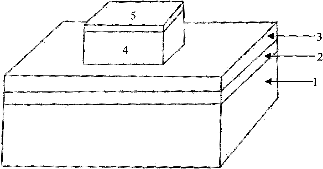
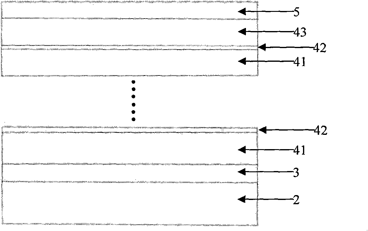
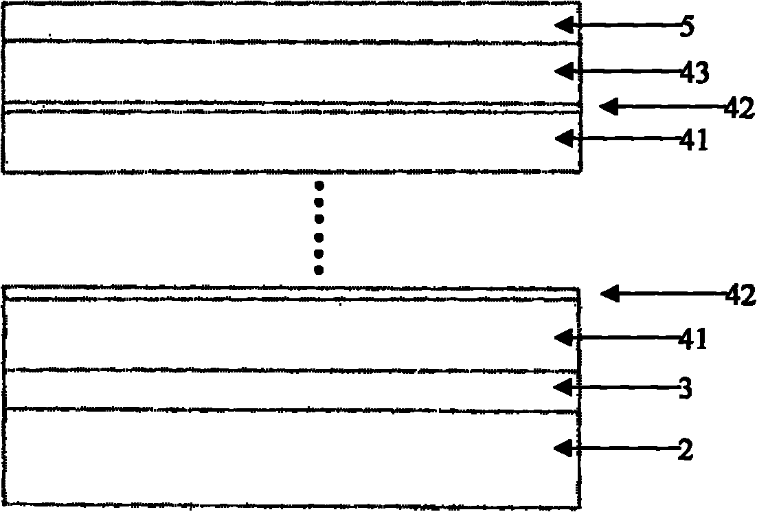
[0024] Such as figure 1 and figure 2 As shown, the quantum well infrared detector proposed by the present invention utilizes GaAs material as the substrate 1, and utilizes MBE or MOCVD technology to grow the following multilayer structure layer by layer:
[0025] (1) One layer of undoped GaAs buffer layer 2 .
[0026] (2) The n-type doped GaAs lower electrode layer 3 has a thickness of 0.5-10 μm, and the dopant is silicon (Si), and its doping concentration is 0.5-5.0×10 18 cm -3 , such as making the Si doping concentration about 1×10 18 cm -3 .
[0027] (3) The multi-quantum well layer 4 formed by alternately growing the potential barrier first and then the potential well in multiple periods, and the number of periods of the multi-quantum well layer 4 is 15-20. Among them, each cycle includes an Al x Ga 1-x As barrier layer 41 and a GaAs potential well layer 42, n-type doping is carried out in the GaAs potential well layer 42, the dopant is Si, and the doping concentr...
PUM
| Property | Measurement | Unit |
|---|---|---|
| Thickness | aaaaa | aaaaa |
Abstract
Description
Claims
Application Information