Method for manufacturing quadri-junction GaInP/GaAs/InGaAs/Ge solar cells

A technology of a solar cell and a manufacturing method, applied in the field of solar photovoltaic, can solve the problems of increasing the difficulty of the battery process, decreasing the battery efficiency, high battery cost, etc., and achieving the effects of improving the photoelectric conversion efficiency, reducing the thermal energy loss, and improving the efficiency.

Inactive Publication Date: 2010-10-13
SUZHOU INST OF NANO TECH & NANO BIONICS CHINESE ACEDEMY OF SCI
View PDF3 Cites 27 Cited by
  • Summary
  • Abstract
  • Description
  • Claims
  • Application Information

AI Technical Summary

Problems solved by technology

Therefore, it is necessary to obtain a thin layer of Ge before bonding, which will greatly increase the process difficulty of battery development.
In addition, in order to reduce the high bat

Method used


Image

  • Method for manufacturing quadri-junction GaInP/GaAs/InGaAs/Ge solar cells
  • Method for manufacturing quadri-junction GaInP/GaAs/InGaAs/Ge solar cells

Examples


Embodiment Construction

[0020] In order to make the above-mentioned purposes, features and advantages of the present invention more obvious and easy to understand, the specific embodiments of the present invention will be described in detail below:

[0021] 1) Cell growth before bonding

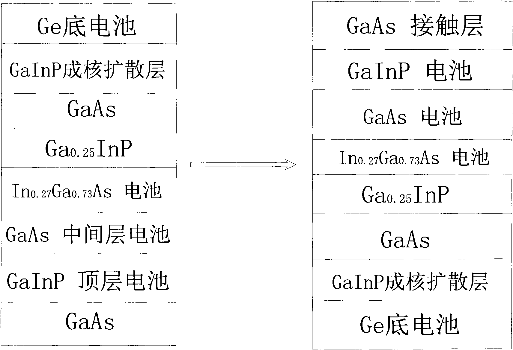
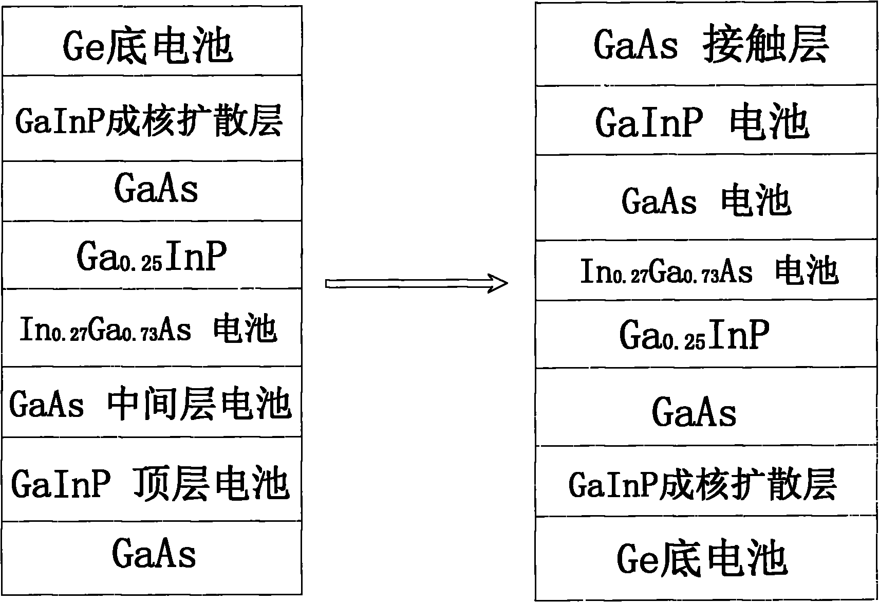
[0022] Such as figure 1 As shown, it is a schematic diagram of the cell structure conversion before and after bonding of the triple-junction GaInP / GaAs / InGaAs solar cell and the single-junction Ge solar cell used in the present invention. It can be clearly seen from the attached figure that the triple-junction cell adopts an inverted growth method, and first grows Ga on the GaAs substrate. 0.51 InP, then GaAs, and finally In 0.27 Ga 0.73 As. The advantage of this is that there is only one interface lattice mismatch. Compared with the direct growth of InGaAs on GaAs, an interface mismatch will be added, that is, between InGaAs and GaAs substrate and between the GaAs battery in the middle. How to effectively tran...


PUM


Abstract

The invention discloses a method for manufacturing quadri-junction GaInP/GaAs/InGaAs/Ge solar cells. In the method, by adopting a wafer bonding method, triple-junction GaInP/GaAs/InGaA solar cells based on inverted structural growth are integrated with a Ge solar cell uniwafer; and a Ge cell is fully utilized to serve as the basic cell of the four cells and a supporting substrate, thus achieving quadri-junction solar cells with the band-gap energy of 1.9/1.4/1.0/0.67eV, realizing absorption and energy conversion of a solar full-spectrum to a larger extent and obtaining the conversion efficiency above 45%. The method lowers high cost caused by a plurality of different substrates adopted in a mechanical cascade solar cell system as well as complicated optical system and optical loss in an optical integrated battery; and meanwhile the method effectively solves the problem of lattice mismatch of a growth uniwafer quadri-junction cascade semiconductor solar cell material, achieves high voltage and low current output, and lowers resistance consumption in the high-power concentrator cell.

Description

technical field [0001] The invention relates to a photovoltaic storage device utilizing solar energy, in particular to a structural design and device preparation of a four-junction solar cell, belonging to the field of solar photovoltaic technology. Background technique [0002] Stimulated by the energy crisis triggered in the 1970s and driven by the demand for space vehicle energy systems, the field of photovoltaic technology has continuously made breakthroughs. Crystalline silicon solar cells, amorphous silicon solar cells, amorphous silicon thin-film solar cells, III-V compound semiconductor solar cells, II-VI compound semiconductor polycrystalline thin-film solar cells, etc., more and more solar cell technologies are maturing . The continuous improvement of photoelectric conversion efficiency and the continuous reduction of manufacturing costs have enabled photovoltaic technology to be widely used in space and on the ground. Looking back at the development of photovolt...

Claims


Application Information

Patent Timeline
IPC IPC(8): H01L31/18
CPCH01L31/06875Y02E10/544
Inventor 陆书龙董建荣杨辉黄伍桥
Owner SUZHOU INST OF NANO TECH & NANO BIONICS CHINESE ACEDEMY OF SCI
Why Eureka
Try Eureka