Method for producing a compound semiconductor MMIC (Monolithic Microwave Integrated Circuit) chip on silicon substrate
A silicon substrate and compound technology, applied in semiconductor/solid-state device manufacturing, electrical components, circuits, etc., can solve the problems of power dissipation, microwave power transmission, high cost, etc., to ensure mechanical strength, reduce cost, and reduce power loss Effect
- Summary
- Abstract
- Description
- Claims
- Application Information
AI Technical Summary
Problems solved by technology
Method used
Image

Examples
Embodiment 1
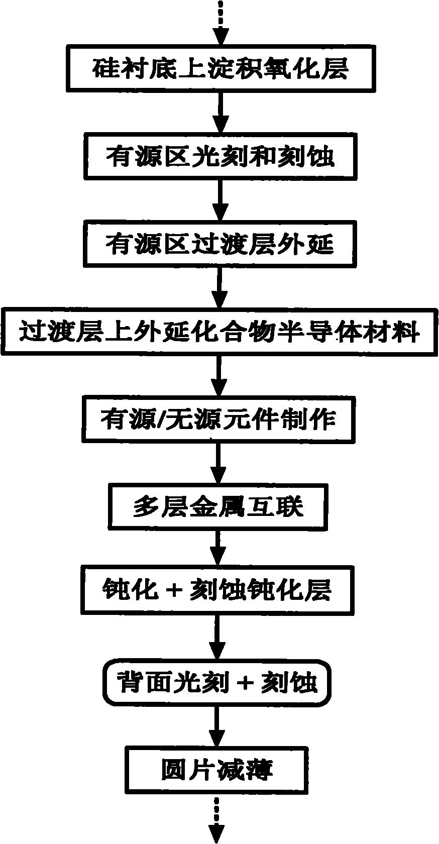
[0039] A kind of technology that prepares compound semiconductor MMIC structure on silicon substrate by dry method, its processing step comprises:
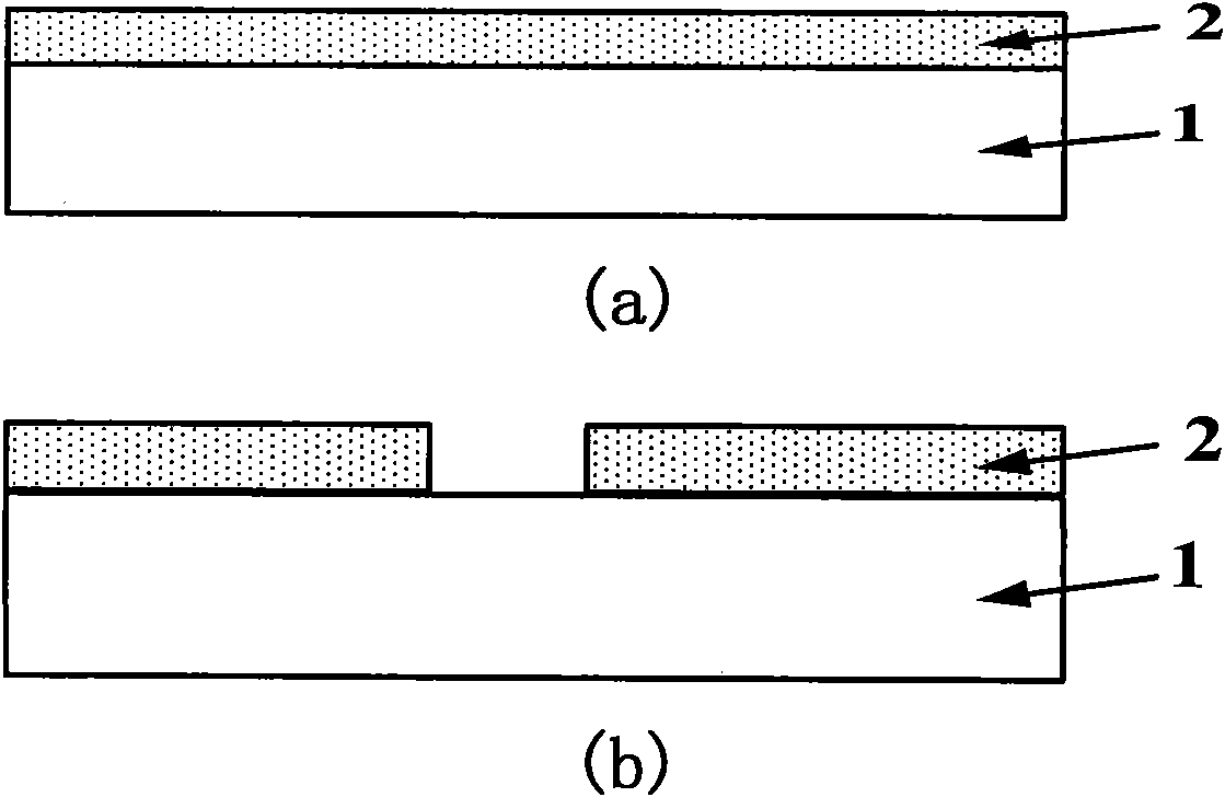
[0040] In the first step, silicon oxide is deposited on the surface of the silicon substrate with a thickness of 300-2000nm.
[0041] In the second step, a window exposing the silicon substrate is obtained by photolithography and etching on the silicon oxide for material growth of active devices.
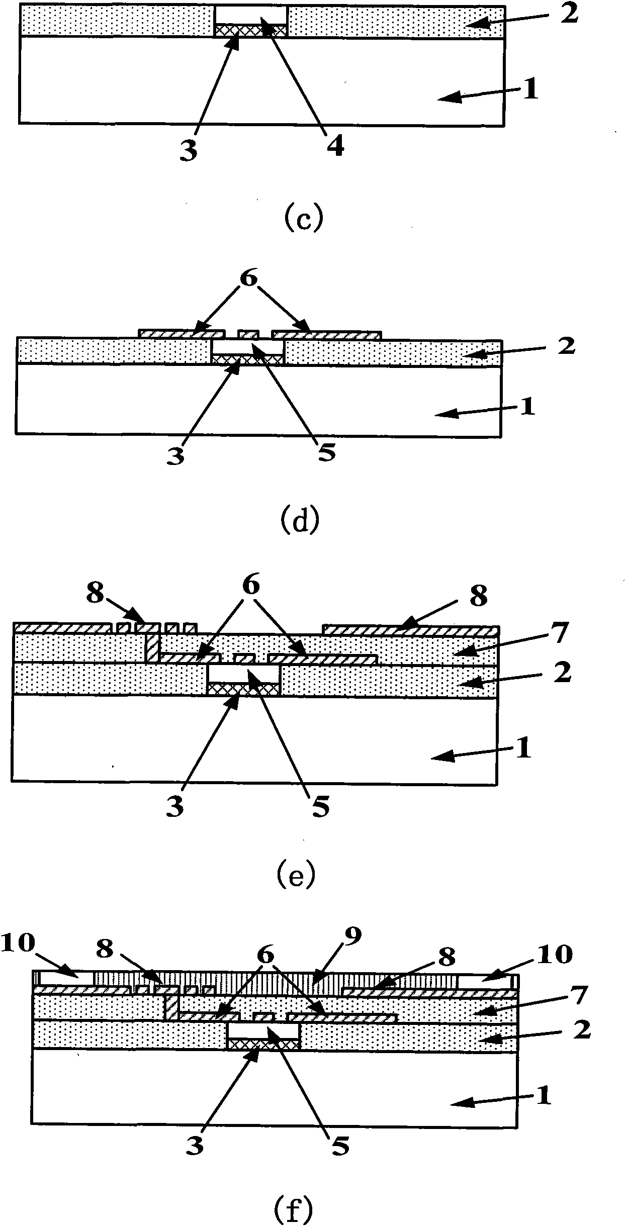
[0042] In the third step, the transition layer and the compound single crystal semiconductor material are grown by selective epitaxy in the window, and the total thickness of the epitaxial layer is the same as that of the oxide layer.
[0043] The fourth step is to make active devices, that is, transistors, from compound single crystal semiconductor materials, and complete the patterning of the first layer of metal. The first layer of metal realizes the functionalization of transistors and is used as the bottom of spiral inductors and c...
Embodiment 2
[0049] A process for preparing compound semiconductor MMIC structures on silicon substrates by wet etching, the process steps comprising:
[0050] In the first step, silicon oxide is deposited on the surface of the silicon substrate with a thickness of 300-2000nm.
[0051] In the second step, a window exposing the silicon substrate is obtained by photolithography and etching on the silicon oxide for material growth of active devices.
[0052]In the third step, the transition layer and the compound single crystal semiconductor material are grown by selective epitaxy in the window, and the total thickness of the epitaxial layer is the same as that of the oxide layer.
[0053] The fourth step is to make active devices, that is, transistors, from compound single crystal semiconductor materials, and complete the patterning of the first layer of metal. The first layer of metal realizes the functionalization of transistors and is used as the bottom of spiral inductors and capacitors....
PUM
 Abstract
Description
Claims
Application Information