Method for manufacturing crystalline silicon high-efficiency solar cell

A technology of solar cells and crystalline silicon, applied in circuits, electrical components, final product manufacturing, etc., can solve the problems of low conversion efficiency and high price, and achieve easy mass production and industrialization, large short-circuit current, and equipment. and the effect of fewer process steps

Active Publication Date: 2010-11-10
锐立平芯微电子(广州)有限责任公司
View PDF0 Cites 7 Cited by
  • Summary
  • Abstract
  • Description
  • Claims
  • Application Information

AI Technical Summary

Problems solved by technology

[0004] At present, the main problems faced by crystalline silicon cells are: the conversion efficiency is not very high (mass production can achieve an average of 17%), the price is expensive, etc.

Method used


Image

  • Method for manufacturing crystalline silicon high-efficiency solar cell
  • Method for manufacturing crystalline silicon high-efficiency solar cell
  • Method for manufacturing crystalline silicon high-efficiency solar cell

Examples


Embodiment Construction

[0033] In order to further set forth the technical means and effects that the present invention takes for reaching the intended purpose of the invention, the specific implementation is described, and the detailed description is as follows:

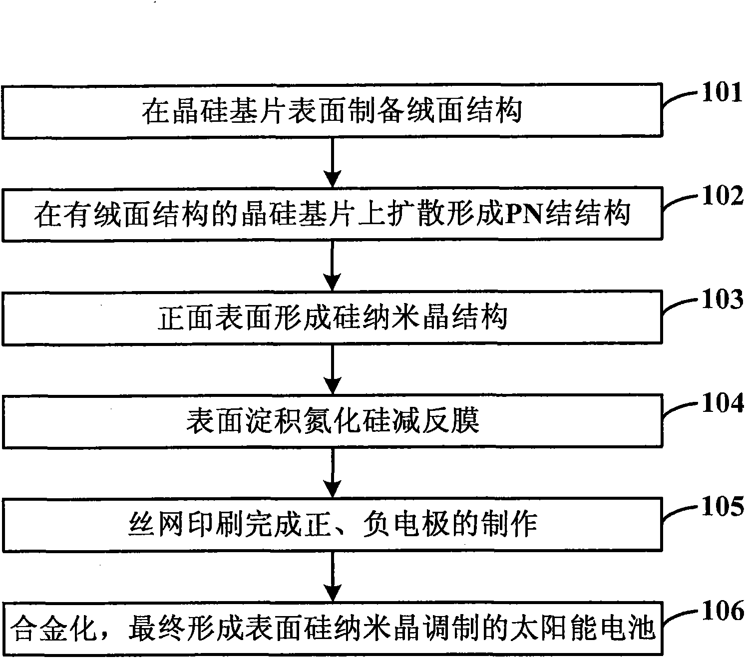
[0034] Such as figure 1 as shown, figure 1 A flow chart of a method for preparing a surface silicon nanocrystal modulated crystalline silicon high-efficiency solar cell provided by the present invention, the method includes the following steps:

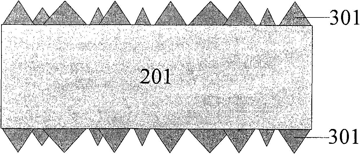
[0035] Step 101: preparing a textured structure on the surface of the crystalline silicon substrate;

[0036] Step 102: Diffusion on a crystalline silicon substrate with a textured structure to form a PN junction structure;

[0037] Step 103: forming a silicon nanocrystal structure on the front surface;

[0038] Step 104: Depositing a silicon nitride antireflection film on the surface;

[0039] Step 105: screen printing to complete the production of positive and negative electrodes;

[0040] ...


PUM

PropertyMeasurementUnit
Thicknessaaaaaaaaaa

Abstract

The invention discloses a method for manufacturing a crystalline silicon high-efficiency solar cell, which comprises: preparing a textured surface structure on the surface of a crystalline silicon substrate; forming a PN junction structure on the crystalline silicon substrate by a diffusion method; forming a silicon nanocrystal structure on the surface by using thin film deposition technology and heat treatment; depositing a silicon nitride antireflective film on the surface of the substrate by using a plasma-reinforced chemical vapor deposition method; making an anode and a cathode by screen printing; and alloying to make the surface silicon nanocrystal modulated solar cell. In the invention, the PN junction crystalline silicon solar cell prepared by a process means used in a mass production is used, silicon nanocrystals are formed on the surface of the PN junction crystalline silicon solar cell, and under the modulating action of the silicon nanocrystals, the crystalline silicon cell can utilize the solar wavelength more effectively to improve the efficiency of the crystalline silicon cell. The method is compatible with the convenient mature large-scale production technology, has the characteristics of simple production process, easy industrialization and the like and can effectively reduce cost and acquire the high-efficiency crystalline silicon solar cell.

Description

technical field [0001] The invention relates to a method for manufacturing crystalline silicon high-efficiency solar cells. The quantum confinement effect of surface silicon nanocrystals is used to modulate light with photon energy greater than the forbidden band width (1.1eV) of bulk silicon, especially short-wavelength light, so that it is crystallized Silicon cells are fully absorbed and utilized to achieve the purpose of improving conversion efficiency and reducing costs. Background technique [0002] In recent years, energy shortages such as rising oil prices and environmental pollution such as global warming have become increasingly serious, and people's demand for clean and renewable energy is unprecedentedly urgent. Solar energy is inexhaustible and is expected to replace traditional energy sources. As an important form of solar energy, solar cells have attracted much attention. [0003] Since Chapin et al first proposed the application of silicon-based PN junction ...

Claims


Application Information

Patent Timeline
IPC IPC(8): H01L31/18
CPCY02P70/50
Inventor 贾锐朱晨昕陈晨李维龙李昊峰张培文刘明刘新宇叶甜春
Owner 锐立平芯微电子(广州)有限责任公司
Why Eureka
Try Eureka